


 Trouble in Your Tank: Understanding Interconnect Defects, Part 1
 It’s Only Common Sense: Marketing Isn’t Fluff, It’s Ammunition
 Driving Innovation: Mechanical and Optical Processes During Rigid-flex Production


Transition from Three to Two Dimensions Increases Conduction
August 5, 2015 | MIPTEstimated reading time: 2 minutes
Scientists from the MIPT Department of Molecular and Chemical Physics have for the first time described the behavior of electrons in a previously unstudied analogue of graphene, two-dimensional niobium telluride, and, in the process, uncovered the nature of two-dimensionality effects on conducting properties. These findings will help in the creation of future flat and flexible electronic devices.
In recent decades, physicists have been actively studying so-called two-dimensional materials. Andrei Geim and Konstantin Novoselov received the Nobel Prize for their research on graphene, the most well-known among them. The properties of such materials, which can be described as “sheets” with a thickness of a few atoms, strongly differ from their three-dimensional analogues. For example, graphene is transparent, conducts current better than copper and has good thermal conductivity. Scientists believe that other types of two-dimensional materials may possess even more exotic properties.
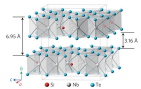
A group of scientists from Russia and the USA, including Pavel Sorokin and Liubov Antipina from MIPT, recently conducted research on the properties of the crystals of one such material,Nb3SiTe6, a compound of niobium telluride. In their structure, the crystals resemble sandwiches with a thickness of three atoms (around 4 angstroms): a layer of tellurium, a layer of niobium mixed with silicon atoms and then another layer of tellurium. This substance belongs to a class of materials known as dichalcogenides, which many scientists view as promising two-dimensional semiconductors.
The scientists synthesized Nb3SiTe6 crystals in a laboratory at Tulane University (New Orleans). They then separated them into two-dimensional layers, taking samples for further analysis by transmission electron microscopy, X-ray crystal analysis and other methods. The goal of the researchers was to investigate electron-phonon interaction changes in two-dimensional substances.
Quasi particles, quanta of crystal lattice oscillations, are called phonons. Physicists introduced the concept of phonons because it helped simplify the description of processes in crystals, and tracking of electron-phonon interaction is fundamentally important for description of the different conducting properties in matter.
"We developed a theory that predicts that electron-phonon interaction is suppressed due to dimensional effects in two-dimensional material. In other words, these materials obstruct the flow of electrons to a lesser extent," says Pavel Sorokin, a co-author of the study, doctor of physical and mathematical sciences, and lecturer at the MIPT Section of the Physics and Chemistry of Nanostructures (DMCP).
American colleagues confirmed this predictioninrelatedexperiments. "They conducted measurements where the same effectwas observed. Our calculations allowed the ruling out of other explanations; we managed to prove that changes in electron-phonon interaction occur specifically because of the two-dimensionality of the membrane," Sorokin adds.
Share on:


Testimonial
"Our marketing partnership with I-Connect007 is already delivering. Just a day after our press release went live, we received a direct inquiry about our updated products!"
Rachael Temple - AlltematedSuggested Items
Trouble in Your Tank: Understanding Interconnect Defects, Part 1
11/04/2025 | Michael Carano -- Column: Trouble in Your TankThis month, I’ll address interconnect defects (ICDs). While this defect continues to rear its ugly head, don’t despair. There are solutions, most of which center on process control and understanding the relationship of the chemistry, materials, and equipment. First, though, let’s discuss ICDs.
WestDev Announces Advanced Thermal Analysis Integration for Pulsonix PCB Design Suite
10/29/2025 | WestDev Ltd.Pulsonix, the industry-leading PCB design software from WestDev Ltd., announced a major enhancement to its design ecosystem: a direct interface between Pulsonix and ADAM Research's TRM (Thermal Risk Management) analysis software.
Designers Notebook: Power and Ground Distribution Basics
10/29/2025 | Vern Solberg -- Column: Designer's NotebookThe principal objectives to be established during the planning stage are to define the interrelationship between all component elements and confirm that there is sufficient surface area for placement, the space needed to ensure efficient circuit interconnect, and to accommodate adequate power and ground distribution.
Episode 6 of Ultra HDI Podcast Series Explores Copper-filled Microvias in Advanced PCB Design and Fabrication
10/15/2025 | I-Connect007I-Connect007 has released Episode 6 of its acclaimed On the Line with... American Standard Circuits: Ultra High Density Interconnect (UHDI) podcast series. In this episode, “Copper Filling of Vias,” host Nolan Johnson once again welcomes John Johnson, Director of Quality and Advanced Technology at American Standard Circuits, for a deep dive into the pros and cons of copper plating microvias—from both the fabricator’s and designer’s perspectives.
Nolan’s Notes: Tariffs, Technologies, and Optimization
10/01/2025 | Nolan Johnson -- Column: Nolan's NotesLast month, SMT007 Magazine spotlighted India, and boy, did we pick a good time to do so. Tariff and trade news involving India was breaking like a storm surge. The U.S. tariffs shifted India from one of the most favorable trade agreements to the least favorable. Electronics continue to be exempt for the time being, but lest you think that we’re free and clear because we manufacture electronics, steel and aluminum are specifically called out at the 50% tariff levels.