


 Facing the Future: The Role of 5G and Beyond in Shaping PCB Demand
 It’s Only Common Sense: Stop Pitching, Start Listening
 Trouble in Your Tank: Causes of Plating Voids, Pre-electroless Copper


Latent Short Circuit Failure in High-Rel PCBs due to Cleanliness of PCB Processes and Base Materials
August 11, 2015 | Stan HeltzelEstimated reading time: 2 minutes

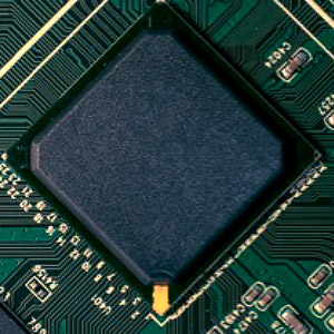
Latent short circuit failures have been observed during testing of PCBs for power distribution of spacecraft of the European Space Agency. Root cause analysis indicates that foreign fibers may have contaminated the PCB laminate. These fibers can provide a pathway for electromigration if they bridge the clearance between nets of different potential in the presence of humidity attracted by the hygroscopic laminate resin. PCB manufacturers report poor yield caused by contamination embedded in laminate. Inspections show that fiber contamination is present on prepreg and etched innerlayers. Further fiber contamination may be attracted in the manufacturing environment due to static charging. The requirements for cleanliness that are specified for final PCBs are orders of magnitude more stringent than
those specified for base materials. This paper describes inspections performed on base materials, manufacturing processes and final PCBs. It describes test methods that detect reduced insulation caused by contamination and electromigration. Moreover, a proposal is presented specifying tightened requirements for a new class of base materials for the manufacture of high-reliability PCBs.
I. Introduction
Latent short circuit failures have been observed in PCBs during testing of power distribution units of spacecraft for the European Space Agency (ESA). Root cause analysis has been conducted under review of non-conformance review boards (NRB). Printed circuit board assemblies failed after prolonged functional testing in ambient laboratory environment or after thermal vacuum cycles. Due to the large amount of damage caused by the electrical overstress, it was not possible to obtain direct evidence of the failure. However, a working hypothesis has been developed indicating that fiber contamination may have caused a latent short circuit. This hypothesis was further substantiated by reports on contamination issues in base materials and by a test method that demonstrated the breach of insulation due to fiber contamination.
At the time of the observed failures at equipment level, PCB manufacturers reported poor cleanliness levels of base laminate materials, causing poor yield. It is not possible to screen in an efficient manner for contamination in copper-clad laminate, since visual inspection requires stripping of the copper. Several inspection methods show the lack of cleanliness of base materials, which is specified in IPC4101[8]. This paper identifies a major gap between the requirements specified on base materials and the requirements on manufactured PCBs and presents a proposal for a new class of cleaner base materials for the manufacture of high-rel PCBs.
Editor's Note: This article originally appeared in the August 2015 issue of The PCB Magazine.
Share on:


Suggested Items
RF PCB Design Tips and Tricks
05/08/2025 | Cherie Litson, EPTAC MIT CID/CID+There are many great books, videos, and information online about designing PCBs for RF circuits. A few of my favorite RF sources are Hans Rosenberg, Stephen Chavez, and Rick Hartley, but there are many more. These PCB design engineers have a very good perspective on what it takes to take an RF design from schematic concept to PCB layout.
Trouble in Your Tank: Causes of Plating Voids, Pre-electroless Copper
05/09/2025 | Michael Carano -- Column: Trouble in Your TankIn the business of printed circuit fabrication, yield-reducing and costly defects can easily catch even the most seasoned engineers and production personnel off guard. In this month’s column, I’ll investigate copper plating voids with their genesis in the pre-plating process steps.
Elephantech: For a Greener Tomorrow
04/16/2025 | Marcy LaRont, PCB007 MagazineNobuhiko Okamoto is the global sales and marketing manager for Elephantech Inc., a Japanese startup with a vision to make electronics more sustainable. The company is developing a metal inkjet technology that can print directly on the substrate and then give it a copper thickness by plating. In this interview, he discusses this novel technology's environmental advantages, as well as its potential benefits for the PCB manufacturing and semiconductor packaging segments.
Trouble in Your Tank: Organic Addition Agents in Electrolytic Copper Plating
04/15/2025 | Michael Carano -- Column: Trouble in Your TankThere are numerous factors at play in the science of electroplating or, as most often called, electrolytic plating. One critical element is the use of organic addition agents and their role in copper plating. The function and use of these chemical compounds will be explored in more detail.
IDTechEx Highlights Recyclable Materials for PCBs
04/10/2025 | IDTechExConventional printed circuit board (PCB) manufacturing is wasteful, harmful to the environment and energy intensive. This can be mitigated by the implementation of new recyclable materials and technologies, which have the potential to revolutionize electronics manufacturing.