


 It’s Only Common Sense: If You’re Not Differentiated, You’re Dead
 Alpha Insights, Performance by Design: The Future of PCB Manufacturing in the Midwest
 Happy’s Tech Talk #43: Engineering Statistics Training With Free Software


Material Moves Foldable Electronics, New Implantable Medical Devices a Step Closer
September 22, 2015 | University of HoustonEstimated reading time: 3 minutes
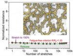
Researchers have discovered a new stretchable, transparent conductor that can be folded or stretched and released, resulting in a large curvature or a significant strain, at least 10,000 times without showing signs of fatigue.
This is a crucial step in creating a new generation of foldable electronics - think a flat-screen television that can be rolled up for easy portability - and implantable medical devices. The work, published Monday in the Proceedings of the National Academy of Sciences, pairs gold nanomesh with a stretchable substrate made with polydimethylsiloxane, or PDMS.
The substrate is stretched before the gold nanomesh is placed on it - a process known as "prestretching" - and the material showed no sign of fatigue when cyclically stretched to a strain of more than 50 percent.
The gold nanomesh also proved conducive to cell growth, indicating it is a good material for implantable medical devices.
Fatigue is a common problem for researchers trying to develop a flexible, transparent conductor, making many materials that have good electrical conductivity, flexibility and transparency - all three are needed for foldable electronics - wear out too quickly to be practical, said Zhifeng Ren, a physicist at the University of Houston and principal investigator at the Texas Center for Superconductivity, who was the lead author for the paper.
The new material, produced by grain boundary lithography, solves that problem, he said.
In addition to Ren, other researchers on the project included Chuan Fei Guo and Ching-Wu "Paul" Chu, both from UH; Zhigang Suo, Qihan Liu and Yecheng Wang, all from Harvard University, and Guohui Wang and Zhengzheng Shi, both from the Houston Methodist Research Institute.
In materials science, "fatigue" is used to describe the structural damage to a material caused by repeated movement or pressure, known as "strain cycling." Bend a material enough times, and it becomes damaged or breaks. That means the materials aren't durable enough for consumer electronics or biomedical devices.
"Metallic materials often exhibit high cycle fatigue, and fatigue has been a deadly disease for metals," the researchers wrote.
"We weaken the constraint of the substrate by making the interface between the Au (gold) nanomesh and PDMS slippery, and expect the Au nanomesh to achieve superstretchability and high fatigue resistance," they wrote in the paper. "Free of fatigue here means that both the structure and the resistance do not change or have little change after many strain cycles."
As a result, they reported, "the Au nanomesh does not exhibit strain fatigue when it is stretched to 50 percent for 10,000 cycles."
Many applications require a less dramatic stretch - and many materials break with far less stretching - so the combination of a sufficiently large range for stretching and the ability to avoid fatigue over thousands of cycles indicates a material that would remain productive over a long period of time, Ren said.
The grain boundary lithography involved a bilayer lift-off metallization process, which included an indium oxide mask layer and a silicon oxide sacrificial layer and offers good control over the dimensions of the mesh structure.
The researchers used mouse embryonic fibroblast cells to determine biocompatibility; that, along with the fact that the stretchability of gold nanomesh on a slippery substrate resembles the bioenvironment of tissue or organ surfaces, suggest the nanomesh "might be implanted in the body as a pacemaker electrode, a connection to nerve endings or the central nervous system, a beating heart, and so on," they wrote.
Ren's lab reported the mechanics of making a new transparent and stretchable electric material, using gold nanomesh, in a paper published in Nature Communications in January 2014.
This work expands on that, producing the material in a different way to allow it to remain fatigue-free through thousands of cycles.
Share on:


Testimonial
"We’re proud to call I-Connect007 a trusted partner. Their innovative approach and industry insight made our podcast collaboration a success by connecting us with the right audience and delivering real results."
Julia McCaffrey - NCAB GroupSuggested Items
Beyond Thermal Conductivity: Exploring Polymer-based TIM Strategies for High-power-density Electronics
10/13/2025 | Padmanabha Shakthivelu and Nico Bruijnis, MacDermid Alpha Electronics SolutionsAs power density and thermal loads continue to increase, effective thermal management becomes increasingly important. Rapid and efficient heat transfer from power semiconductor chip packages is essential for achieving optimal performance and ensuring long-term reliability of temperature-sensitive components. This is particularly crucial in power systems that support advanced applications such as green energy generation, electric vehicles, aerospace, and defense, along with high-speed computing for data centers and artificial intelligence (AI).
Is Glass Finally Coming of Age?
10/13/2025 | Nolan Johnson, I-Connect007Substrates, by definition, form the base of all electronic devices. Whether discussing silicon wafers for semiconductors, glass-and-epoxy materials in printed circuits, or the base of choice for interposers, all these materials function as substrates. While other substrates have come and gone, silicon and FR-4 have remained the de facto standards for the industry.
Creative Materials to Showcase Innovative Functional Inks for Medical Devices at COMPAMED 2025
10/09/2025 | Creative Materials, Inc.Creative Materials, a leading manufacturer of high-performance functional inks and coatings, is pleased to announce its participation in COMPAMED 2025, taking place November 17–20 in Düsseldorf, Germany.
Jiva Leading the Charge Toward Sustainable Innovation
09/30/2025 | Marcy LaRont, PCB007 MagazineEnvironmental sustainability in business—product circularity—is a high priority these days. “Circularity,” the term meant to replace “recycling,” in its simplest definition, describes a full circle life for electronic products and all their elements. The result is re-use or a near-complete reintroduction of the base materials back into the supply chain, leaving very little left for waste. For what cannot be reused productively, the ultimate hope is to have better, less harmful means of disposal and/or materials that can seamlessly and harmlessly decompose and integrate back into the natural environment. That is where Jiva and Soluboard come in.
Space Forge Inc. and United Semiconductors LLC Partner to Develop the Supply Chain for Space-grown Semiconductor Materials
09/29/2025 | Space Forge Inc.Space Forge Inc., the advanced materials company revolutionizing semiconductor manufacturing in space, has announced the signing of a strategic Memorandum of Understanding (MoU) with United Semiconductors LLC, a leading specialist in bulk crystal growth of III-V semiconductor compounds. The agreement formalizes the ongoing collaborative efforts that started over a year ago, marking a significant step forward in strengthening the partnership between the two companies.