


 Driving Innovation: Mechanical and Optical Processes During Rigid-flex Production
 It’s Only Common Sense: Your Biggest Competitor Is Complacency
 The Chemical Connection: Onshoring PCB Production—Daunting but Certainly Possible


DuPont Displays Opens OLED Materials Scale-Up Facility for Next Generation TVs
September 30, 2015 | DuPont DisplaysEstimated reading time: 2 minutes
DuPont Displays today announced the opening of a state-of-the-art, scale-up manufacturing facility designed to deliver production scale quantities of advanced materials that enable large-format, solution-based printed Organic Light Emitting Diode (OLED) displays. These materials are designed to help manufacturers develop OLED displays that are brighter, more vivid, longer lasting and significantly less expensive than the OLED TVs on the market today. The facility is located at the DuPont Stine-Haskell Research Center (Stine-Haskell) in Newark, Del., near DuPont’s global headquarters in Wilmington.
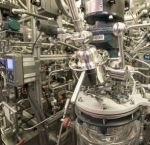
Jim Collins, executive vice president, DuPont, tours the new OLED materials scale-up facility at Stine-Haskell with Avi Avula, global business director, DuPont Displays.
DuPont’s new OLED materials scale-up facility at Stine-Haskell is designed to deliver production scale quantities of advanced materials that enable large-format, solution-based printed OLED displays.
DuPont’s new OLED facility at Stine-Haskell has large-scale formulation systems and can support simultaneous production of multiple product lines.
“Materials are critical to the performance of an OLED TV and we are confident that DuPont has the best performing solution OLED materials available in the market today,” said Avi Avula, global business director, DuPont Displays. “Our vision is that OLEDs will become the display standard and to make that vision a reality, we are focused on helping our customers bring the cost of large sized OLED TVs down to less than $1000 by 2020.”
DuPont’s new scale-up facility is sized to meet the future growth expectations of the OLED TV industry, which analysts predict will increase by over 70 percent for the next several years and will require large quantities of highly sophisticated OLED materials. DuPont has been developing its suite of advanced OLED materials for the last 15 years. These materials are highly regarded for both solution and evaporative applications due to their long lifetime and deep color. In addition to its recently announced collaboration with an inkjet equipment maker to advance solution printed displays, DuPont is actively engaged with the leading OLED display manufacturers to bring solution printed OLED technology to market as quickly as possible.
DuPont’s new OLED facility at Stine-Haskell has large-scale formulation systems and can support simultaneous production of multiple product lines. It was designed with a focus on employee safety, environmental responsibility and producing superior quality materials with the highest possible purity. The project was partially funded by a grant from the state of Delaware in 2012, with DuPont investing more than $20 million in the facility.
DuPont Displays brings more than 15 years of experience in enabling evaporative and solution-based OLED technologies through advanced materials that deliver the color, efficiency and lifetime performance that display manufacturers and consumers demand. DuPont offers highly engineered, next-generation OLED materials as well as solution process know-how that makes the promise of lower cost OLED technology commercially feasible for TVs and other large-format displays.
About DuPont
DuPont has been bringing world-class science and engineering to the global marketplace in the form of innovative products, materials, and services since 1802. The company believes that by collaborating with customers, governments, NGOs, and thought leaders we can help find solutions to such global challenges as providing enough healthy food for people everywhere, decreasing dependence on fossil fuels, and protecting life and the environment.
Share on:


Testimonial
"Our marketing partnership with I-Connect007 is already delivering. Just a day after our press release went live, we received a direct inquiry about our updated products!"
Rachael Temple - AlltematedSuggested Items
Sealed for Survival: Potting Electronics for the Toughest Environments
10/29/2025 | Beth Massey, MacDermid Alpha Electronics SolutionsElectronics deployed in harsh conditions face relentless threats from vibration, impact, chemical contaminants, airborne pollutants, and moisture, conditions that can quickly lead to failure without robust protection. Potting, the process of encapsulating electronics in a protective polymer, is a widely used strategy to safeguard devices from both environmental and mechanical hazards.
Driving Innovation: Mechanical and Optical Processes During Rigid-flex Production
10/28/2025 | Kurt Palmer -- Column: Driving InnovationRigid-flex printed circuit boards are a highly effective solution for placing complex circuitry in tight, three-dimensional spaces. They are now indispensable across a range of industries, from medical devices and aerospace to advanced consumer electronics, helping designers make the most efficient use of available space. However, their unique construction—combining rigid and flexible materials—presents a fundamental challenge for PCB manufacturers.
SMTAI 2025 Review: Reflecting on a Pragmatic and Forward-looking Industry
10/27/2025 | Marcy LaRont, I-Connect007Leaving the show floor on the final afternoon of SMTA International last week in Rosemont, Illinois, it was clear that the show remains a grounded, technically driven event that delivers a solid program, good networking, and an easy space to commune with industry colleagues and meet with customers.
ITW EAE Despatch Ovens Now Support ASTM 5423 Testing
10/15/2025 | ITW EAEAs the demand for high-performance electrical insulation materials continues to grow—driven by the rapid expansion of electric vehicles (EVs) and energy storage systems—thermal processing has become a critical step in material development.
Beyond Thermal Conductivity: Exploring Polymer-based TIM Strategies for High-power-density Electronics
10/13/2025 | Padmanabha Shakthivelu and Nico Bruijnis, MacDermid Alpha Electronics SolutionsAs power density and thermal loads continue to increase, effective thermal management becomes increasingly important. Rapid and efficient heat transfer from power semiconductor chip packages is essential for achieving optimal performance and ensuring long-term reliability of temperature-sensitive components. This is particularly crucial in power systems that support advanced applications such as green energy generation, electric vehicles, aerospace, and defense, along with high-speed computing for data centers and artificial intelligence (AI).