


 Beyond the Board: How a Diminished Supplier Base Affects Complex PCB Manufacturing Readiness in Defense
 Defense Speak Interpreted: Hypersonics Report Back After Six Years of Silence
 American Made Advocacy: American Microelectronics Power the Future of High Technology


Liquid Cooling Moves Onto the Chip for Denser Electronics
October 5, 2015 | Georgia Institute of TechnologyEstimated reading time: 4 minutes
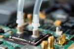
Using microfluidic passages cut directly into the backsides of production field-programmable gate array (FPGA) devices, Georgia Institute of Technology researchers are putting liquid cooling right where it's needed the most - a few hundred microns away from where the transistors are operating.
Combined with connection technology that operates through structures in the cooling passages, the new technologies could allow development of denser and more powerful integrated electronic systems that would no longer require heat sinks or cooling fans on top of the integrated circuits. Working with popular 28-nanometer FPGA devices made by Altera Corp., the researchers have demonstrated a monolithically-cooled chip that can operate at temperatures more than 60 percent below those of similar air-cooled chips.
In addition to more processing power, the lower temperatures can mean longer device life and less current leakage. The cooling comes from simple de-ionized water flowing through microfluidic passages that replace the massive air-cooled heat sinks normally placed on the backs of chips.
"We believe we have eliminated one of the major barriers to building high-performance systems that are more compact and energy efficient," said Muhannad Bakir, an associate professor and ON Semiconductor Junior Professor in the Georgia Tech School of Electrical and Computer Engineering. "We have eliminated the heat sink atop the silicon die by moving liquid cooling just a few hundred microns away from the transistors. We believe that reliably integrating microfluidic cooling directly on the silicon will be a disruptive technology for a new generation of electronics."
Supported by the Defense Advanced Research Projects Agency (DARPA), the research is believed to be the first example of liquid cooling directly on an operating high-performance CMOS chip. Details of the research were presented on September 28 at the IEEE Custom Integrated Circuits Conference in San Jose, Calif.
Liquid cooling has been used to address the heat challenges facing computing systems whose power needs have been increasing. However, existing liquid cooling technology removes heat using cold plates externally attached to fully packaged silicon chips - adding thermal resistance and reducing the heat-rejection efficiency.
To make their liquid cooling system, Bakir and graduate student Thomas Sarvey removed the heat sink and heat-spreading materials from the backs of stock Altera FPGA chips. They then etched cooling passages into the silicon, incorporating silicon cylinders approximately 100 microns in diameter to improve heat transmission into the liquid. A silicon layer was then placed over the flow passages, and ports were attached for the connection of water tubes.
In multiple tests - including a demonstration for DARPA officials in Arlington, Virginia - a liquid-cooled FPGA was operated using a custom processor architecture provided by Altera. With a water inlet temperature of approximately 20 degrees Celsius and an inlet flow rate of 147 milliliters per minute, the liquid-cooled FPGA operated at a temperature of less than 24 degrees Celsius, compared to an air-cooled device that operated at 60 degrees Celsius.
Sudhakar Yalamanchili, a professor in the Georgia Tech School of Electrical and Computer Engineering and one of the research group's collaborators, joined the team for the DARPA demonstration to discuss electrical-thermal co-design.
"We have created a real electronic platform to evaluate the benefits of liquid cooling versus air cooling," said Bakir. "This may open the door to stacking multiple chips, potentially multiple FPGA chips or FPGA chips with other chips that are high in power consumption. We are seeing a significant reduction in the temperature of these liquid-cooled chips."
The research team chose FPGAs for their test because they provide a platform to test different circuit designs, and because FPGAs are common in many market segments, including defense. However, the same technology could also be used to cool CPUs, GPUs and other devices such as power amplifiers, Bakir said.
In addition to improving overall cooling, the system could reduce hotspots in circuits by applying cooling much closer to the power source. Eliminating the heat sink could allow more compact packaging of electronic devices - but only if electrical connection issues are also addressed.
In a separate research project, Bakir's group has demonstrated the fabrication of copper vias that would run through the silicon columns that are part of the cooling structure fabricated on the FPGAs. Graduate student Hanju Oh, co-advised with College of Engineering Dean Gary May, fabricated high aspect ratio copper vias through the silicon columns, reducing the capacitance of the connections that would carry signals between chips in an array.
"The moment you start thinking about stacking the chips, you need to have copper vias to connect them," Bakir said. "By bringing system components closer together, we can reduce interconnect length and that will lead to improvements in bandwidth density and reductions in energy use."
The cooling research was funded by DARPA's Microsystems Technology Office, through the ICECOOL program. At Georgia Tech, DARPA funds two major cooling and system integration projects, one called STAECool directed by George W. Woodruff School of Mechanical Engineering Professor Yogendra Joshi, and the other, called SuperCool, that is directed by Bakir. In collaboration with the STAECool effort, Bakir and Joshi, along with Professors Andrei Fedorov and Suresh Sitaraman from the School of Mechanical Engineering, developed a thermal design vehicle to emulate challenging power maps to test the benefits of microfluidic cooling.
"We have reached an important milestone that we hope to use as a stepping stone to reach other objectives," said Bakir. "There is still a big challenge ahead, but we expect this to allow much denser, higher-performance computing systems that will dissipate less power. We can think of many interesting applications for these cooling technologies."
Altera's principal investigator for the project, Arifur Rahman, said: "Future high-performance semiconductor electronics will be increasingly dominated by thermal budget and ability to remove heat. The embedded microfluidic channels provide an intriguing option to remove heat from future microelectronics systems."
This research was supported by DARPA-MTO; the contents of the news release are the responsibility of the authors and do not necessarily reflect the official position of DARPA.
Share on:


Testimonial
"The I-Connect007 team is outstanding—kind, responsive, and a true marketing partner. Their design team created fresh, eye-catching ads, and their editorial support polished our content to let our brand shine. Thank you all! "
Sweeney Ng - CEE PCBSuggested Items
Nortech Systems Launches Power over Fiber Technology Platform for EMI-Sensitive Applications
04/08/2026 | Globe NewswireNortech Systems Incorporated, a leading provider of design and manufacturing solutions for complex electromedical devices and electromechanical systems, has announced the launch of its Power over Fiber technology platform.
Flexible Thinking: Designing Flex Circuits for Dynamic Reliability
04/09/2026 | Joe Fjelstad -- Column: Flexible ThinkingFlex circuits flex. No surprises there. However, they are also very commonly designed into products because they are thin and offer consistent thickness and dielectric properties, attributes highly prized by present-day product designers of personal electronics. This would include smartphones and, increasingly, wearable electronics for medical monitoring and even fashion.
Understanding Tolerances in Flexible Circuit Design
04/01/2026 | Chris Clark, Flexible Circuit TechnologiesThe challenge with cumulative tolerances is meeting the dimensional requirements for items dimensioned on a drawing or specification for a flexible or rigid-flex circuit. It is critical to understand the fabrication processes and how features are defined when creating your tolerance requirements.
Target Condition: An Exploration of Flooding PCB Layers
04/02/2026 | Kelly Dack -- Column: Target ConditionThe concept of flooding PCB layers with copper has been around for so long, you’d think we’d have it mastered. We haven’t. (Oh, and by “we,” I mean design engineers and the software tools we depend on.) Years ago, PCB artwork was created by hand using light tables, with tape applied to Mylar. Signals were slow, traces were relatively wide, and high-current paths were simply “beefed up” with wider copper. Signal integrity wasn’t yet a driving concern. Today, solid return paths are fundamental to robust design. We understand the importance of continuous reference planes for signal integrity and EMI control.
New, Greener Solutions for Etch: Novel Copper Extraction
03/30/2026 | Richard Nichols, GreenSource Engineering“Novel” is a typical marketing phrase that implies new and unique, but often “novel” actually means an established technology being applied to a new field or application. This, in turn, is often driven by newly relevant external motivation. GreenSource has been working on just such a solution: novel copper extraction, offering a better and greener alternative to traditional LLE control systems for cupric chloride etch.