


 Trouble in Your Tank: Understanding Interconnect Defects, Part 1
 It’s Only Common Sense: Marketing Isn’t Fluff, It’s Ammunition
 Driving Innovation: Mechanical and Optical Processes During Rigid-flex Production


New Acoustic Technique Reveals Structural Information in Nanoscale Materials
December 29, 2015 | Georgia Institute of TechnologyEstimated reading time: 4 minutes
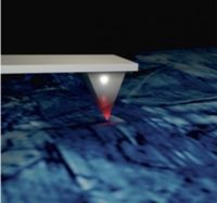
Understanding where and how phase transitions occur is critical to developing new generations of the materials used in high-performance batteries, sensors, energy-harvesting devices, medical diagnostic equipment and other applications. But until now there was no good way to study and simultaneously map these phenomena at the relevant length scales.
Now, researchers at the Georgia Institute of Technology and Oak Ridge National Laboratory (ORNL) have developed a new nondestructive technique for investigating these material changes by examining the acoustic response at the nanoscale. Information obtained from this technique - which uses electrically-conductive atomic force microscope (AFM) probes - could guide efforts to design materials with enhanced properties at small size scales.
The approach has been used in ferroelectric materials, but could also have applications in ferroelastics, solid protonic acids and materials known as relaxors. Sponsored by the National Science Foundation and the Department of Energy's Office of Science, the research was reported December 15 in the journal Advanced Functional Materials.
"We have developed a new characterization technique that allows us to study changes in the crystalline structure and changes in materials behavior at substantially smaller length scales with a relatively simple approach," said Nazanin Bassiri-Gharb, an associate professor in Georgia Tech's Woodruff School of Mechanical Engineering. "Knowing where these phase transitions happen and at which length scales can help us design next-generation materials."
In ferroelectric materials such as PZT (lead zirconate titanate), phase transitions can occur at the boundaries between one crystal type and another, under external stimuli. Properties such as the piezoelectric and dielectric effects can be amplified at the boundaries, which are caused by the multi-element "confused chemistry" of the materials. Determining when these transitions occur can be done in bulk materials using various techniques, and at the smallest scales using an electron microscope.
Page 1 of 2
Share on:


Testimonial
"In a year when every marketing dollar mattered, I chose to keep I-Connect007 in our 2025 plan. Their commitment to high-quality, insightful content aligns with Koh Young’s values and helps readers navigate a changing industry. "
Brent Fischthal - Koh YoungSuggested Items
SEMI Foundation Honors Applied Materials at SEMICON West with 2025 Excellence in Achievement Award for Talent Development
11/04/2025 | SEMIThe SEMI Foundation announced it recognized Applied Materials, Inc. with the Excellence in Achievement Award at SEMICON West 2025 in Phoenix, Arizona, honoring the company’s outstanding leadership and collaboration in building the next generation of semiconductor talent.
On the Line With… Ultra HDI, Episode 8: “Materials, Up and Coming Capabilities,” Now Available
11/05/2025 | I-Connect007I-Connect007 is excited to announce the release of the eighth episode of its 12-part podcast series, On the Line With… American Standard Circuits: Ultra HDI. In this episode, “Materials, Up and Coming Capabilities,” host Nolan Johnson sits down with resident expert John Johnson, Director of Quality and Advanced Technology at American Standard Circuits, to discuss how material selection influences the Ultra HDI (UHDI) manufacturing process.
New Podcast Episode: “Bonding Innovation: How Adhesives and Coatings Are Powering the Next Generation of Electronics”
11/05/2025 | I-Connect007I-Connect007 has released of a new episode in its Voices of the Industry podcast series, titled “Bonding Innovation: How Adhesives and Coatings Are Powering the Next Generation of Electronics.” Hosted by Nolan Johnson, this insightful discussion dives deep into the evolving world of adhesives and coatings—materials that are redefining performance, reliability, and design in modern electronics manufacturing. Dymax's Doug Katze, a leading expert in adhesive technologies, delivers what can only be described as a master class on how these critical materials are adapting to meet rapidly changing market demands.
Sealed for Survival: Potting Electronics for the Toughest Environments
10/29/2025 | Beth Massey, MacDermid Alpha Electronics SolutionsElectronics deployed in harsh conditions face relentless threats from vibration, impact, chemical contaminants, airborne pollutants, and moisture, conditions that can quickly lead to failure without robust protection. Potting, the process of encapsulating electronics in a protective polymer, is a widely used strategy to safeguard devices from both environmental and mechanical hazards.
Driving Innovation: Mechanical and Optical Processes During Rigid-flex Production
10/28/2025 | Kurt Palmer -- Column: Driving InnovationRigid-flex printed circuit boards are a highly effective solution for placing complex circuitry in tight, three-dimensional spaces. They are now indispensable across a range of industries, from medical devices and aerospace to advanced consumer electronics, helping designers make the most efficient use of available space. However, their unique construction—combining rigid and flexible materials—presents a fundamental challenge for PCB manufacturers.