


 The Right Approach: I Hear the Train A Comin'
 It’s Only Common Sense: OCCAM—the Time Is Now
 Marcy's Musings: The Growing Industry
World's Largest Flexible X-Ray Detector
December 31, 2015 | Arizona State UniversityEstimated reading time: 1 minute
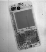
The Flexible Electronics and Display Center (FEDC) at Arizona State University and PARC, a Xerox company, announced that they have successfully manufactured the world's largest flexible X-ray detector prototypes using advanced thin film transistors.
Measuring 10 diagonal inches, the device has been jointly developed at the ASU center and PARC in conjunction with the Army Research Lab and the Defense Threat Reduction Agency. The device will be used to advance the development of flexible X-ray detectors for use in thin, lightweight, conformable and highly rugged devices.
"This achievement is a fantastic example of how academia, industry and government can collaborate to advance key technologies and national priorities," said Sethuraman "Panch" Panchanathan, senior vice president for Knowledge Enterprise Development at ASU.
"Flexible electronics hold tremendous potential to accelerate our global competitiveness in the area of advanced manufacturing by partnering with federal agencies and industry leaders."
The thin film transistor and PIN diode processing was done on the 470- by 370-mm Gen II line at the Flexible Electronics and Display Center. This device showcases the center's successful scale up to GEN II, and the ability to produce sensors and displays using thin film transistors in standard process flows with the center's proprietary bond/de-bond technology. These detectors are unique in that they showcase both of the flexible substrates the center uses to make devices. Some of the new detectors are on polyethylene naphthalate and some are on polyimide. Printed and Flexible Sensors 2015-2025 "This success came from a rewarding collaboration that combines FEDC's flexible array fabrication technology and PARC's experience with digital X-ray systems," said Bob Street, PARC Senior Research Fellow.
The system design and integration was done at PARC. The flexible X-ray sensor was coupled to a tablet device for control and image viewing. This system shows PARC's capability to build user-defined prototype systems incorporating novel device physics, materials and technology. PARC has extensive experience in building large-area electronic systems, display and backplane prototypes, and organic and printed electronics.
Share on:


Suggested Items
Warm Windows and Streamlined Skin Patches – IDTechEx Explores Flexible and Printed Electronics
04/26/2024 | IDTechExFlexible and printed electronics can be integrated into cars and homes to create modern aesthetics that are beneficial and easy to use. From luminous car controls to food labels that communicate the quality of food, the uses of this technology are endless and can upgrade many areas of everyday life.
Book Excerpt: The Printed Circuit Assembler’s Guide to... Factory Analytics
04/24/2024 | I-Connect007 Editorial TeamIn our fast-changing, deeply competitive, and margin-tight industry, factory analytics can be the key to unlocking untapped improvements to guarantee a thriving business. On top of that, electronics manufacturers are facing a tremendous burden to do more with less. If you don't already have a copy of this book, what follows is an excerpt from the introduction chapter of 'The Printed Circuit Assembler’s Guide to... Factory Analytics: Unlocking Efficiency Through Data Insights' to whet your appetite.
Listen Up! The Intricacies of PCB Drilling Detailed in New Podcast Episode
04/25/2024 | I-Connect007In episode 5 of the podcast series, On the Line With: Designing for Reality, Nolan Johnson and Matt Stevenson continue down the manufacturing process, this time focusing on the post-lamination drilling process for PCBs. Matt and Nolan delve into the intricacies of the PCB drilling process, highlighting the importance of hole quality, drill parameters, and design optimization to ensure smooth manufacturing. The conversation covers topics such as drill bit sizes, aspect ratios, vias, challenges in drilling, and ways to enhance efficiency in the drilling department.
Elevating PCB Design Engineering With IPC Programs
04/24/2024 | Cory Blaylock, IPCIn a monumental stride for the electronics manufacturing industry, IPC has successfully championed the recognition of the PCB Design Engineer as an official occupation by the U.S. Department of Labor (DOL). This pivotal achievement not only underscores the critical role of PCB design engineers within the technology landscape, but also marks the beginning of a transformative journey toward nurturing a robust, skilled workforce ready to propel our industry into the future.
Winner of The Science Show Rakett 69 Receives Incap Scholarship
04/24/2024 | IncapThe winner of the Rakett 69 science show, Andri Türkson, who stood out as an electronics enthusiast, received a scholarship from Incap Estonia, along with an internship opportunity in Saaremaa.