


 The Right Approach: The Pros and Cons of PCB Vertical Integration
 American Made Advocacy: PCBAA’s Fifth Annual Meeting—Growing Membership and Valuable Relationships
 It's Only Common Sense: Why the Best Years of Electronics Are Still Ahead of Us


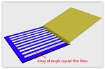
For fabrication of organic ferroelectric devices, one of the problems to be solved is to make a homogeneous thin film. The developed printing technique that stimulates thin-film formation from a solution allows formation of highly uniform single-crystalline thin films of organic ferroelectrics. The thin-film device fabricated by the developed technique worked as a memory device with only 3 V which is lower than operation voltage of various memory devices. The developed technique is expected to accelerate the research and development on low power consumption device of printed electronics such as ferroelectric memories and nonvolatile semiconductor FETs.
Details of the results will soon be published online in a German scientific journal, Advanced Materials.
Schematic of fabrication process of single-crystalline thin films of organic ferroelectric molecules
Social Background of Research
Active R&D of the "printed electronics", which applies printing technologies to the production of electronic devices by forming precise, high-quality, metallic and/or semiconducting patterns, has been conducted globally. So far, several printing methods have been enthusiastically developed to fabricate metallic wires and semiconductor layers for transistors, although the development of printing techniques for other types of materials has not been conducted enough. Ferroelectric materials could reduce the power consumption of electronic devices such as ferroelectric memories in IC cards and nonvolatile semiconductor FETs. Therefore, it is required to develop patterning techniques for ferroelectric thin films though printing technologies.
Ferroelectric materials are generally composed of inorganic materials so that it was considered to be difficult to apply a printing process. Although organic ferroelectric polymer materials are applicable to a printing process, their ferroelectric characteristics are inferior to those of inorganic materials. In recent years, research and development of organic ferroelectrics composed of small molecules have advanced. Some new organic materials showing superior characteristics comparable to inorganic ones have been found. Though thin-film formation of these materials is indispensable for making them into devices, it is difficult to form thin films of the materials. Therefore, it was desired to develop a fabrication technique of uniform thin film without any pinholes through a printing process.
Page 1 of 3


