


 Punching Out: Breaking Out of the Valuation Box
 Happy’s Tech Talk #28: The Power Mesh Architecture for PCBs
 It’s Only Common Sense: Would You Join Your Own Company?
Nanoelectronics Scores Laboratory Victory
November 10, 2016 | New York UniversityEstimated reading time: 2 minutes
Researchers at the NYU Tandon School of Engineering have pioneered a method for growing an atomic scale electronic material at the highest quality ever reported. In a paper published in Applied Physics Letters ("Electronic Properties of Monolayer Tungsten Disulfide Grown by Chemical Vapor Deposition"), Assistant Professor of Electrical and Computer Engineering Davood Shahrjerdi and doctoral student Abdullah Alharbi detail a technique for synthesizing large sheets of high-performing monolayer tungsten disulfide, a synthetic material with a wide range of electronic and optoelectronic applications.
"We developed a custom reactor for growing this material using a routine technique called chemical vapor deposition. We made some subtle and yet critical changes to improve the design of the reactor and the growth process itself, and we were thrilled to discover that we could produce the highest quality monolayer tungsten disulfide reported in the literature," said Shahrjerdi. "It's a critical step toward enabling the kind of research necessary for developing next-generation transistors, wearable electronics, and even flexible biomedical devices."
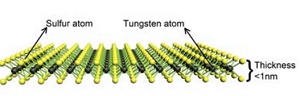
At just one atom thick, tungsten disulfide allows energy to switch off and on -- important for nano-scale electronic transistors -- but it also absorbs and emits light, which could find applications in optoelectronics, sensing, and flexible electronics. The NYU logo shows the monolayer material emitting light. Researchers at NYU Tandon reported success in growing the promising monolayer material. (click on image to enlarge)
At just one atom thick, tungsten disulfide allows energy to switch off and on -- important for nano-scale electronic transistors -- but it also absorbs and emits light, which could find applications in optoelectronics, sensing, and flexible electronics. The NYU logo shows the monolayer material emitting light. Researchers at NYU Tandon reported success in growing the promising monolayer material.
The promise of two-dimensional electronic materials has tantalized researchers for more than a decade, since the first such material — graphene — was experimentally discovered. Also called "monolayer" materials, graphene and similar two-dimensional materials are a mere one atom in thickness, several hundred thousand times thinner than a sheet of paper. These materials boast major advantages over silicon — namely unmatched flexibility, strength, and conductivity — but developing practical applications for their use has been challenging.
Graphene (a single layer of carbon) has been explored for electronic switches (transistors), but its lack of an energy band gap poses difficulties for semiconductor applications. "You can't turn off the graphene transistors," explained Shahrjerdi. Unlike graphene, tungsten disulfide has a sizeable energy band gap. It also displays exciting new properties: When the number of atomic layers increases, the band gap becomes tunable, and at monolayer thickness it can strongly absorb and emit light, making it ideal for applications in optoelectronics, sensing, and flexible electronics.
Efforts to develop applications for monolayer materials are often plagued by imperfections in the material itself — impurities and structural disorders that can compromise the movement of charge carriers in the semiconductor (carrier mobility). Shahrjerdi and his student succeeded in reducing the structural disorders by omitting the growth promoters and using nitrogen as a carrier gas rather than a more common choice, argon.
Shahrjerdi noted that comprehensive testing of their material revealed the highest values recorded thus far for carrier mobility in monolayer tungsten disulfide. "It's a very exciting development for those of us doing research in this field," he said.
Share on:


Suggested Items
Ansys’ Collaboration with Schrödinger will Accelerate Materials Development with Unprecedented Multiscale Simulation
05/09/2024 | ANSYSAnsys and Schrödinger are collaborating to deliver an ICME approach that bridges the gap between materials discovery and product development.
2024 Apple iPad Pro Estimated to Ship Between 4.5 to 5 Million Units
05/08/2024 | TrendForceApple’s recent product launch in May introduced a lineup of new tablets featuring advanced AMOLED screens. Notably, the Pro version boasts a dual-layer tandem structure designed to address the longstanding challenges of screen burn-in and lifespan that are common with AMOLED displays.
AIM Solder Signs Shinil Fl Ltd. as New Distributor for Korea
05/08/2024 | AIM SolderAIM Solder, a leading global manufacturer of solder assembly materials for the electronics industry, is pleased to announce a new distribution partnership with Shinil Fl Ltd., a prominent supplier of technological solutions in the SMT and semiconductor sectors.
IDTechEx Discusses Low-Loss Materials: The Enabler of Future Connected Vehicles?
05/06/2024 | IDTechExFuture connected vehicles will offer future drivers a safer, smoother, and more convenient driving experience. Not only will drivers get access to more navigation and entertainment options, but they will also gain access to safety technologies that will potentially reduce accidents, improve congestion, and reduce emissions globally by allowing vehicle safety systems to communicate with each other and with city traffic infrastructure.
LQDX Divests Aluminum Soldering Business - Mina™ - to Taiyo America Inc.
05/02/2024 | PRNewswireLQDX, formerly known as Averatek Corp., developer of high-performance materials for advanced semiconductor manufacturing, today announced that it has divested its aluminum soldering business – known as MinaTM – to Taiyo America Inc., a global market leader in advanced electronic materials.