


 Punching Out: Breaking Out of the Valuation Box
 Happy’s Tech Talk #28: The Power Mesh Architecture for PCBs
 It’s Only Common Sense: Would You Join Your Own Company?
Diamonds - The Ultimate Semiconductors
November 29, 2016 | Tokyo Institute of TechnologyEstimated reading time: 6 minutes
"While we think of diamonds as very expensive jewelry, they can actually be made using methane and hydrogen. Diamonds are really just carbon, a light and simple element. Their simple yet unique characteristics create significant potential for use in a wide range of purposes, including generation of environmental energy and biological applications," says Professor Mutsuko Hatano.
Diamonds, although nonconductive, can be altered to function as semiconductors with the addition of phosphorus and boron. Silicon, the most common semiconductor, is widely used in memory devices and microprocessors. It is also used in power devices. As power devices are key for social infrastructure that facilitates smart grids, high capacity is required. As a result, the demand for high-capacity power production with minimal loss during power conversion calls for the development of new semiconductor materials.
The thermal conductivity of diamonds is 14 times greater than that of silicon, and electrical field resistance is 30 times greater. High thermal conductivity allows the release of heat, which can reduce the size of cooling systems normally required during the generation of increased levels of electric power. High electrical field resistance suppresses power conversion losses. With these characteristics, diamonds are the ultimate semiconductors for electronic devices that require several kilovolts (kV) of power, such as those used in electric vehicles, railways, and power transmission.
Although the formation of diamond-based n-type semiconductors, whose conduction carriers are electrons, and p-type semiconductors, whose conduction carriers are electron holes, has been achieved, the difficulty has traditionally lain in the formation of the lateral p-n junction, which is the basic structure of devices. Collaborating with researchers at the National Institute of Advanced Industrial Science and Technology, Hatano established a lateral p-n junction, which was then applied to a junction field effect transistor (FET) prototype. This was the world's first high-voltage power device, whose application to power supply optimization in smart grids is significantly reducing environmental impact.
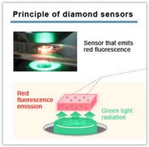
Diamond sensor with high potential for biological applications
Hatano is now focusing on the development of a diamond sensor, which has attracted attention around the world due to its potential application to biology.
In a diamond crystal, carbon atoms can be replaced by nitrogen atoms to create nitrogen-vacancy complexes (NV centers). Negatively charged NV centers exhibit a magnetic property called electron spin*. Green light radiation causes the emission of red fluorescence. Depending on the magnetic field, fluorescence processes change, and magnetic field strength and direction can be detected. Diamond sensors apply these characteristics, and the imaging of a magnetic field is enabled.
Diamond sensors are superior to other sensors because they allow a wider range of spatial resolution — from nanometers to millimeters — and have a high magnetic sensitivity. Another outstanding characteristic is that while SQUID magnetic sensors conventionally require a low temperature, diamond sensors operate at room temperature.
Diamond sensors enable scalable application to spatial resolution, which is required for the nanometer-level analysis of protein structures, submicron cell measurement applied to drug delivery and immunological testing, and micron-level analysis of medical imaging, medicines, foods, and noninvasive measurement.
Hatano wants to address issues in both the dynamic use of diamond sensors in power device semiconductors and the application of diamond sensors at the nanoscale. In order to do so, she facilitates integration of research in areas such as the life sciences, theoretical physics, materials sciences, and her specialty — electronics and electrical engineering — and promotes collaboration with overseas researchers.
Massive impact of cooperation in the United States
Hatano's research on diamonds is an outgrowth of her general interest in science, something that was sparked during her early childhood. On her fourth birthday, she received Virginia Lee Burton's Life Story from her grandfather. This children's story of the history of Earth impressed her deeply. Hatano's parents both have science backgrounds, and she often talked with her father about things such as which atoms made up the food they were having for dinner. She was also excited by the experiments in her elementary school science class. The professor looks back happily on her childhood. She says that the educational environment at home and school worked well for her, considering Japan's need to compete globally in the field of science and technology in order to compensate for its lack of natural resources.
At Hitachi, Ltd., where she was hired after graduating from university, Hatano was engaged in fundamental research on superconductivity and quantum effect devices for 12 years. During her employment, she also earned her doctorate. She then worked as a project leader in research and development for the commercialization of mobile displays, and projects related to environmental energy electronics.
Hitachi sent her to participate in joint research at University of California, Berkeley (UCB) for three years in 1997. That experience had a great impact on her way of thinking and approach to research. Her specialty was electronics, but she chose to collaborate with a professor specializing in machine engineering. Through the accumulation of research on heat, they deepened their mutual understanding and discovered a new field, something that was extremely meaningful for her.
"Coming from different backgrounds, our discussions had a synergistic effect that led to the establishment of a new field. Changing specializations and jobs is common in Silicon Valley. Through such mobility, technology and know-how are expanded to a wide range of locations. This leads to the establishment of new startup companies," Hatano says.
The professor was exposed to a wide range of stimuli living in a different culture. When she moved to UCB, her firstborn was an elementary school student while her second daughter was in nursery school. At that time, Silicon Valley was experiencing its peak period of new startups. The elementary school attended by her first daughter had students from over ten different countries, reminding Hatano that Silicon Valley was attracting specialists from around the world. The infrastructure, however, was struggling to keep up with the rapid growth in population, and schools had reached capacity. In an effort to counter this, Hatano was involved in the establishment of a new elementary school in cooperation with other companies in the region — HP Inc., Xerox Parc, and numerous startups. Some of the classes were taught by employees from universities, NASA, and major enterprises.
"My daughter's classmate's mother was a professor at Stanford University. She dissected a cow's eye for the students, which wowed everyone. Until then, my daughters had only had the chance to dissect frogs, making that an unforgettable experience for them," Hatano reminisces.
Opening new doors with scrap and build
"I came to Tokyo Tech with a clean slate," Hatano says.
The professor moved from Hitachi Ltd. to Tokyo Tech in July 2010, a change she made after deciding to shift her focus to education. Although her work at Hitachi was fulfilling and secure, she chose a completely different environment because she dislikes complacency, opting instead to follow a scrap-and-build life. At first, she felt the stark contrast between private enterprise and university. Sharing her struggle with students, however, she was able to show that, regardless of the occasional ups and downs, anyone could start from zero at any time.
Hatano has a message for Tokyo Tech students. "It has become increasingly important to create new and innovative value rather than simply focus on problem solving. Tokyo Tech students should apply their knowledge to the creation of new value and the design of a new society through cooperation with people specializing in a wide range of fields. With mutual understanding and cooperative competition, things that you simply can't create alone emerge."
To conclude, Hatano reveals a secret. When producing artificial diamonds for sensors, some diamonds become pink. We are not exactly sure why this happens. Naturally colored diamonds are rare and sell for incredibly high prices overseas. In 2013, a 59-carat pink diamond sold for 8.3 billion yen. "I dream of being surrounded by diamonds one day, like 007," Hatano smiles. Her research continues.
Share on:


Suggested Items
Real Time with… IPC APEX EXPO 2024: Direct Imaging Equipment and Quad-wave DLP Light Engine Technology
05/03/2024 | Real Time with...IPC APEX EXPOGuest Editor Kelly Dack and MivaTek's Brendan Hogan delve into the company's innovative technologies, including direct imaging equipment and quad-wave DLP light engine technology. They highlight the benefits of direct imaging, compensation, and DART technology.
Merlin Flex invests in New Schmoll Direct Imaging System
04/30/2024 | Merlin Flex LtdMerlin Flex has fully installed and commissioned its 2nd Schmoll MDI Direct Imaging system. This new machine includes a twin bed, 4 head system which enhances Merlin Flex’s direct imaging capability for its 1.4M long flexible circuits.
Inkjet Solder Mask ‘Has Arrived’
04/10/2024 | Pete Starkey, I-Connect007I was delighted to be invited to attend an interactive webinar entitled “Solder Mask Coating Made Easy with Additive Manufacturing,” hosted by SUSS MicroTec Netherlands in Eindhoven. The webinar was introduced and moderated by André Bodegom, managing director at Adeon Technologies, and the speakers were Mariana Van Dam, senior product manager PCB imaging solutions at AGFA in Belgium; Ashley Steers, sales manager at Electra Polymers in the UK; and Dr. Luca Gautero, product manager at SUSS MicroTec Netherlands.
NetVia Group Acquires Direct Imaging from Mivatek
04/09/2024 | Miva TechnologiesMiva Technologies is pleased to announce NetVia Group, Irving, TX has acquired a new Miva 2400NG Dual Tray Direct Imaging System with 30-micron capabilities for inner, outer and soldermask imaging.
Teledyne to Acquire Adimec
02/13/2024 | TeledyneTeledyne Technologies Incorporated announced that it has entered into an agreement to acquire Adimec Holding B.V. and its subsidiaries.