


 American Made Advocacy: What About the Rest of the Technology Stack?
 It’s Only Common Sense: Great Ideas From John Mitchell’s Book on Hiring Habits
 Punching Out: Breaking Out of the Valuation Box
Polycrystalline Materials in Solar Cells Gain New Impulse With Findings From INL Researchers
January 30, 2017 | INLEstimated reading time: 1 minute
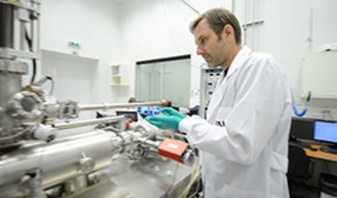
The conversion of sunlight into electricity through solar cells is considered to be a future cornerstone in a renewable energy supply for a sustainable society. The semiconducting compound Cu(In,Ga)Se2, which is deposited as a thin polycrystalline layer onto a metallized glass carrier, has long been known as an excellent light absorber. In the last 5 years, the power conversion efficiency of solar cells based on this material has reached new record values, from ~19.8% in 2011 to 22.6% in 2016, within reach of those of the commercially dominating silicon wafer technology. These recent advances have been achieved through the introduction of a potassium-fluoride treatment of the Cu(In,Ga)Se2 material. It is generally assumed that this treatment mainly affects the region of and near the charge-separating interface.
Researchers of the International Iberian Nanotechnology Laboratory (INL) in Braga have now demonstrated that also the electronic properties of the grain boundaries between the grains of the light absorbing layer are beneficially affected by the potassium treatment.
The study was performed in collaboration with researchers from the Institut des Matériaux Jean Rouxel (IMN) from the University of Nantes, who fabricated the solar cell samples and was published today in Scientific Reports, Effect of the KF post-deposition treatment on grain boundary properties in Cu(In, Ga)Se2 thin films an open access journal published by the Nature Group.
The researchers used an advanced scanning probe microscopy method to image electronic surface properties with nanometer-scale spatial resolution. “We were able to show that the potassium treatment results in a stronger and more homogeneous electronic effect at the grain boundaries” says Nicoleta Nicoara, member of the Laboratory of Nanostructured Solar Cells at INL involved in the research. Polycrystalline semiconductor materials can usually be fabricated more cost-efficient at lower processing temperatures compared to single-crystalline materials. However, the presence of grain boundaries limits their use in many applications, as they lead to losses in performance due to the presence of defects. Sascha Sadewasser who led this study summarizes: “Our study demonstrates that the potassium fluoride treatment can beneficially modify the properties of grain boundaries in Cu(In,Ga)Se2 solar cell materials. The insight we gained through our study might well influence research directions in other polycrystalline materials, and animate researcher to search for treatments with similarly positive effects on the electronic properties of grain boundaries”.
Share on:


Suggested Items
The Shaughnessy Report: Unlock Your High-speed Material Constraints
05/15/2024 | Andy Shaughnessy -- Column: The Shaughnessy ReportThe world of PCB materials used to be a fairly simple one. It was divided into two groups: the “traditional” laminates, often called FR-4, and the high-speed laminates developed especially for high-speed PCBs. These were two worlds that usually didn’t collide. But then traditional laminates started getting better, and high-speed designers and design engineers took notice and started to reconsider what FR-4 could be used for.
Breaking High-speed Material Constraints: Design007 Magazine — May 2024
05/14/2024 | I-Connect007 Editorial TeamDo you need specialty materials for your high-speed designs? Maybe not. Improvements in resins mean designers of high-speed boards can sometimes use traditional laminate systems instead of high-speed materials, saving time and money while streamlining the fab process. In the May 2024 issue of Design007 Magazine, our contributors explain how to avoid overconstraining your materials when working with high-speed boards.
Indium Experts to Present at Electronics in Harsh Environments SMTA Conference
05/13/2024 | Indium Corporationndium Corporation Technical Manager for Europe, Africa, and the Middle East, Karthik Vijay, will deliver a technical presentation and Indium Corporation Senior Technologist, Dr. Ronald Lasky, will deliver both a workshop and technical presentation at the Electronics in Harsh Environments SMTA Conference on May 14-16 in Copenhagen, Denmark.
Ansys’ Collaboration with Schrödinger will Accelerate Materials Development with Unprecedented Multiscale Simulation
05/09/2024 | ANSYSAnsys and Schrödinger are collaborating to deliver an ICME approach that bridges the gap between materials discovery and product development.
2024 Apple iPad Pro Estimated to Ship Between 4.5 to 5 Million Units
05/08/2024 | TrendForceApple’s recent product launch in May introduced a lineup of new tablets featuring advanced AMOLED screens. Notably, the Pro version boasts a dual-layer tandem structure designed to address the longstanding challenges of screen burn-in and lifespan that are common with AMOLED displays.