


 American Made Advocacy: What About the Rest of the Technology Stack?
 It’s Only Common Sense: Great Ideas From John Mitchell’s Book on Hiring Habits
 Punching Out: Breaking Out of the Valuation Box
Thin, Flexible, Light-Absorbent Material for Energy and Stealth Applications
February 2, 2017 | UC San DiegoEstimated reading time: 3 minutes
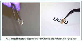
Transparent window coatings that keep buildings and cars cool on sunny days. Devices that could more than triple solar cell efficiencies. Thin, lightweight shields that block thermal detection. These are potential applications for a thin, flexible, light-absorbing material developed by engineers at the University of California San Diego.
The material, called a near-perfect broadband absorber, absorbs more than 87 percent of near-infrared light (1,200 to 2,200 nanometer wavelengths), with 98 percent absorption at 1,550 nanometers, the wavelength for fiber optic communication. The material is capable of absorbing light from every angle. It also can theoretically be customized to absorb certain wavelengths of light while letting others pass through.
Materials that “perfectly” absorb light already exist, but they are bulky and can break when bent. They also cannot be controlled to absorb only a selected range of wavelengths, which is a disadvantage for certain applications. Imagine if a window coating used for cooling not only blocked infrared radiation, but also normal light and radio waves that transmit television and radio programs.
By developing a novel nanoparticle-based design, a team led by professors Zhaowei Liu and Donald Sirbuly at the UC San Diego Jacobs School of Engineering has created a broadband absorber that’s thin, flexible and tunable. The work was published online on Jan. 24 in Proceedings of the National Academy of Sciences.
“This material offers broadband, yet selective absorption that could be tuned to distinct parts of the electromagnetic spectrum,” Liu said.
The absorber relies on optical phenomena known as surface plasmon resonances, which are collective movements of free electrons that occur on the surface of metal nanoparticles upon interaction with certain wavelengths of light. Metal nanoparticles can carry a lot of free electrons, so they exhibit strong surface plasmon resonance — but mainly in visible light, not in the infrared.
UC San Diego engineers reasoned that if they could change the number of free electron carriers, they could tune the material’s surface plasmon resonance to different wavelengths of light. “Make this number lower, and we can push the plasmon resonance to the infrared. Make the number higher, with more electrons, and we can push the plasmon resonance to the ultraviolet region,” Sirbuly said. The problem with this approach is that it is difficult to do in metals.
To address this challenge, engineers designed and built an absorber from materials that could be modified, or doped, to carry a different amount of free electrons: semiconductors. Researchers used a semiconductor called zinc oxide, which has a moderate number of free electrons, and combined it with its metallic version, aluminum-doped zinc oxide, which houses a high number of free electrons — not as much as an actual metal, but enough to give it plasmonic properties in the infrared.
The materials were combined and structured in a precise fashion using advanced nanofabrication technologies in the Nano3 cleanroom facility at the Qualcomm Institute at UC San Diego. The materials were deposited one atomic layer at a time on a silicon substrate to create an array of standing nanotubes, each made of alternating concentric rings of zinc oxide and aluminum-doped zinc oxide. The tubes are 1,730 nanometers tall, 650 to 770 nanometers in diameter, and spaced less than a hundred nanometers apart. The nanotube array was then transferred from the silicon substrate to a thin, elastic polymer. The result is a material that is thin, flexible and transparent in the visible.
“There are different parameters that we can alter in this design to tailor the material’s absorption band: the gap size between tubes, the ratio of the materials, the types of materials, and the electron carrier concentration. Our simulations show that this is possible,” said Conor Riley, a recent nanoengineering Ph.D. graduate from UC San Diego and the first author of this work. Riley is currently a postdoctoral researcher in Sirbuly’s group.
Those are just a few exciting features of this particle-based design, researchers said. It’s also potentially transferrable to any type of substrate and can be scaled up to make large surface area devices, like broadband absorbers for large windows. “Nanomaterials normally aren’t fabricated at scales larger than a couple centimeters, so this would be a big step in that direction,” Sirbuly said.
The technology is still at the developmental stage. Liu and Sirbuly’s teams are continuing to work together to explore different materials, geometries and designs to develop absorbers that work at different wavelengths of light for various applications.
Share on:


Suggested Items
The Shaughnessy Report: Unlock Your High-speed Material Constraints
05/15/2024 | Andy Shaughnessy -- Column: The Shaughnessy ReportThe world of PCB materials used to be a fairly simple one. It was divided into two groups: the “traditional” laminates, often called FR-4, and the high-speed laminates developed especially for high-speed PCBs. These were two worlds that usually didn’t collide. But then traditional laminates started getting better, and high-speed designers and design engineers took notice and started to reconsider what FR-4 could be used for.
Breaking High-speed Material Constraints: Design007 Magazine — May 2024
05/14/2024 | I-Connect007 Editorial TeamDo you need specialty materials for your high-speed designs? Maybe not. Improvements in resins mean designers of high-speed boards can sometimes use traditional laminate systems instead of high-speed materials, saving time and money while streamlining the fab process. In the May 2024 issue of Design007 Magazine, our contributors explain how to avoid overconstraining your materials when working with high-speed boards.
Indium Experts to Present at Electronics in Harsh Environments SMTA Conference
05/13/2024 | Indium Corporationndium Corporation Technical Manager for Europe, Africa, and the Middle East, Karthik Vijay, will deliver a technical presentation and Indium Corporation Senior Technologist, Dr. Ronald Lasky, will deliver both a workshop and technical presentation at the Electronics in Harsh Environments SMTA Conference on May 14-16 in Copenhagen, Denmark.
Ansys’ Collaboration with Schrödinger will Accelerate Materials Development with Unprecedented Multiscale Simulation
05/09/2024 | ANSYSAnsys and Schrödinger are collaborating to deliver an ICME approach that bridges the gap between materials discovery and product development.
2024 Apple iPad Pro Estimated to Ship Between 4.5 to 5 Million Units
05/08/2024 | TrendForceApple’s recent product launch in May introduced a lineup of new tablets featuring advanced AMOLED screens. Notably, the Pro version boasts a dual-layer tandem structure designed to address the longstanding challenges of screen burn-in and lifespan that are common with AMOLED displays.