


 The Chemical Connection: Reducing Etch System Water Usage, Part 2
 It’s Only Common Sense: Nice Guys Really Can Finish First
 The Right Approach: I Hear the Train A Comin'
'Editing' New Metamaterials Brings Light Into Focus
February 14, 2017 | University of California - BerkeleyEstimated reading time: 3 minutes
As cell phones have become smaller, so have their camera lenses. Phones thinner than a cut deck of cards now capture images so sharp that they can be blown up beyond movie-poster size.
When arrayed in nano-scale thin sheets, a familiar compound can be selectively heated to transform part of it into a metal yet leave the remainder transparent, an innovation that provides a range of potential applications. Photo: Peg Skorpinski
But the camera’s convex lenses impose an inherent limit on how thin the phone can be. With more than a billion-plus cell phones bought last year, manufacturers faced an unwelcome choice: either make a thicker camera or sacrifice the quality of the photos.
Now, another type of lens may be emerging, one with light-focusing power that does away with the classic convex piece of glass or plastic. Instead, it relies on “metamaterials” — fabricated arrays of nano-structures so named because they perform unlike any other natural substances.
Metamaterials are made of millions of nano-scale particles, each about the size of a virus. Although the particles themselves are made of atoms, their novel effects on material’s performance have earned them the name “artificial atoms.”
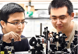
Materials scientist Jie Yao is developing a technique to fabricate one such metamaterial into a new form with strong commercial potential. He can transform a natural phase change material in a way that seems like alchemy, turning some sections of the material into metal but leaving others unchanged.
The metallic portions can interact with light as if they were nanoscale antennas, and Yao has shown that in certain conformations, the combined effect of tens of thousands of these antennas can focus light like a lens.
With support from the Bakar Fellows Program, his lab in the materials science and engineering department is fabricating nano-thin sheets of phase change material. The material is glass-like at room temperature but becomes metallic when heated slightly. Using a local heat source, Yao is able to convert part of the thin sheets into the metal antennas while letting other parts remain transparent.
The interactions of the nano-antennas with light are so effective that films hundreds of times thinner than a conventional lens could tightly control the path of light that passes through the film, Yao says.
He intends to refine his technology’s novel ability to tweak the metallic components’ 3-D shape, and he hopes to open up a range of applications to control visible light as well as infrared and microwave wavelengths.
“The metallic phase change material is the working part of the material, while the insulating part provides the matrix to hold the ‘artificial atoms’ in place,” Yao says.
“When a broad beam of light hits the array, it can be considered as composed of many finer beams. Each new beam passes by an antenna, which is able to change its unique path.
“Using a local heat source, we can ‘write’ new structures into the material. Then, by lowering the temperature, we can erase and re-write them. We can change the material’s structure, and performance at will. No complicated nano-fabrication process is needed.”
By using this etch-a-sketch local heating strategy, his team can change the material’s configuration in real time — potentially in less than a second. “In this we may be able to create a dynamic optical device, for example, a single lens whose focus can be changed whenever necessary,” Yao says.
The array can be “written” in such a way that each antenna will guide light to the same focal point to form a lens. The next moment, the array can be erased and a new array may be written, and the focal point changed to another location, which could be used to improve the performance of photography and other imaging processes.
Beyond the vision of new lenses for a billion cell phones, the technology’s ability to control visible light could yield-thin computer or wall displays. In principle, Yao says, the material and the transforming technique can yield conformations to manipulate infrared light, or microwave radiation as well, leading to novel types of infrared sensors and other optical devices.
“The material is a platform that allows us to draw any photonic structure, so we really can achieve a range of applications and transform them from static devices to dynamic ones.”
Share on:


Suggested Items
LQDX Divests Aluminum Soldering Business - Mina™ - to Taiyo America Inc.
05/02/2024 | PRNewswireLQDX, formerly known as Averatek Corp., developer of high-performance materials for advanced semiconductor manufacturing, today announced that it has divested its aluminum soldering business – known as MinaTM – to Taiyo America Inc., a global market leader in advanced electronic materials.
Indium Corporation Expert to Present on Pb-Free Solder for Die-Attach in Discrete Power Applications
04/30/2024 | Indium CorporationIndium Corporation Product Manager – Semiconductor Dean Payne will present at the Advanced Packaging for Power Electronics conference, hosted by IMAPS, held May 8-9 in Woburn, Massachusetts, USA.
Real Time with... IPC APEX EXPO 2024: Adhesive Materials and Equipment Update with Dymax
05/01/2024 | Real Time with...IPC APEX EXPOVirginia Hogan, global business development manager at Dymax, discusses adhesive materials, dispensing and curing equipment, a new, high-reliability conformal coating, and various materials and dispensing methods.
Real Time with... IPC APEX EXPO 2024: Sustainability in the Industry
04/26/2024 | Real Time with...IPC APEX EXPOGuest Editor Henry Crandall and Chris Nash of Indium Corporation discuss the company's 90th anniversary and its focus on sustainability. They focus on the benefits of sustainable materials, their compatibility, and value propositions. The conversation also highlights how Durafuse LT technology's role in reducing reflow temperatures is leading to significant cost and energy savings. Nash also touches on downstream sustainability efforts such as using recycled materials for packaging.
SMC Korea 2024 to Highlight Semiconductor Materials Trends and Innovations on Industry’s Path to $1 Trillion
04/24/2024 | SEMIWith Korea a major consumer of semiconductor materials and advanced materials a key driver of innovation on the industry’s path to $1 trillion, industry leaders and experts will gather at SMC (Strategic Materials Conference) Korea 2024 on May 29 at the Suwon Convention Center in Gyeonggi-do, South Korea to provide insights into the latest materials developments and trends. Registration is open.