


 The Chemical Connection: Reducing Etch System Water Usage, Part 2
 It’s Only Common Sense: Nice Guys Really Can Finish First
 The Right Approach: I Hear the Train A Comin'
Surprising Spin Behavior at Room Temperature
February 17, 2017 | Tokyo Institute of TechnologyEstimated reading time: 2 minutes
Surprising spin behavior at room temperature: circularly polarized room-temperature electroluminescence from spin-polarized light-emitting diodes.
Scientists at Tokyo Institute of Technology have observed almost purely circularly polarized electroluminescence from GaAs-based spin-polarized light-emitting diodes at room temperature, with no external magnetic field. This behavior indicates the presence of spin-dependent nonlinear processes, which may allow the development of semiconductor-based spin-photonic devices in the future.
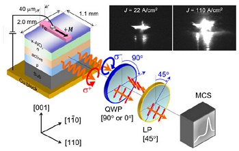
Figure 1. Spin-LED chip placed on a copper block (left) and emitting CP EL (orange spiral arrows); the right- (σ+) and left (σ-)-handed EL components are indicated by the red and blue circles, respectively. QWP, LP, and MCS represent a quarter-wave plate, a linear polarizer, and a multichannel spectrometer, respectively. Inset: EL from a spin-LED chip for different current densities.
The field of spintronics focuses on spin transport behavior in magnetic metals, and the major findings in this area have important implications for the field of electronics. This is because conventional electronics primarily considers the electron charge, whereas spintronics allows the electron spin to be exploited. One of the most significant advancements in spintronics has been the introduction of spin degrees of freedom to semiconductors, which are essential components of modern electronic and photonic applications. However, most experiments investigating spin manipulation in semiconductors have been performed under high magnetic fields and at cryogenic temperatures.
Recently, Specially Appointed Assistant Professor Nozomi Nishizawa and Professor Hiro Munekata and colleagues, from the Institute of Innovative Research, Tokyo Institute of Technology, examined the behavior of spin-polarized light-emitting diodes (LEDs) at room temperature and without an external magnetic field. Hence, they achieved the unexpected result of almost purely circularly polarized (CP) electroluminescence (EL).
The LEDs used in the study contained an epitaxial double heterostructure (sandwich-like structure) of AlGaAs/GaAs/AlGaAs, a crystalline γ-like AlOx tunnel barrier (for electrical stability during operation), and a polycrystalline Fe in-plane spin injector. During operation, spins of a given type were injected into the device. Spin relaxation then caused these spins to disperse and adopt other orthogonal orientations. Radiative recombination subsequently occurred, which was observed in the form of a linearly polarized emission.
Experiments on the LED chips showed that a higher current density generated an increase in the emission intensity. Nishizawa and coworkers also noted that the difference between the left- and right-handed EL components increased with the current density. Specifically, the intensity of the left-handed minority component decreased with increased current density, whereas that of the right-handed majority component increased linearly. Therefore, when the current density was sufficiently high (~100 A/cm2), almost pure CP was achieved. Investigating this behavior in more detail, the researchers found that p-type doping in the active layer allowed the CP observation, which arose from spin-dependent nonlinear processes occurring at a sufficiently high current density.
In the future, higher current densities will be applied in order to elucidate the mechanism behind these nonlinear processes and to investigate the possibility of stimulated CP emission in other geometries. Other important avenues of investigation also exist, e.g., potential spin-LED applications in secure optical communications, cancer diagnosis, and optically enhanced nuclei imaging.
Share on:


Suggested Items
The Chemical Connection: Reducing Etch System Water Usage, Part 2
05/02/2024 | Don Ball -- Column: The Chemical ConnectionIn my last column, I reviewed some relatively simple ways to reduce water usage in existing etch systems: cutting down cooling coil water flow, adding chillers to replace plant water for cooling, lowering flow rate nozzles for rinses, etc. This month, I’ll continue with more ways to control water usage in your etcher. Most of these are not easily retrofittable to existing equipment but should be given serious consideration when new equipment is contemplated. With the right combination of add-ons, it is possible to bring the amount of water used in an etch system to almost zero.
Designer’s Notebook: What Designers Need to Know About Manufacturing, Part 2
04/24/2024 | Vern Solberg -- Column: Designer's NotebookThe printed circuit board (PCB) is the primary base element for providing the interconnect platform for mounting and electrically joining electronic components. When assessing PCB design complexity, first consider the component area and board area ratio. If the surface area for the component interface is restricted, it may justify adopting multilayer or multilayer sequential buildup (SBU) PCB fabrication to enable a more efficient sub-surface circuit interconnect.
Insulectro’s 'Storekeepers' Extend Their Welcome to Technology Village at IPC APEX EXPO
04/03/2024 | InsulectroInsulectro, the largest distributor of materials for use in the manufacture of PCBs and printed electronics, welcomes attendees to its TECHNOLOGY VILLAGE during this year’s IPC APEX EXPO at the Anaheim Convention Center, April 9-11, 2024.
ENNOVI Introduces a New Flexible Circuit Production Process for Low Voltage Connectivity in EV Battery Cell Contacting Systems
04/03/2024 | PRNewswireENNOVI, a mobility electrification solutions partner, introduces a more advanced and sustainable way of producing flexible circuits for low voltage signals in electric vehicle (EV) battery cell contacting systems.
Heavy Copper PCBs: Bridging the Gap Between Design and Fabrication, Part 1
04/01/2024 | Yash Sutariya, Saturn Electronics ServicesThey call me Sparky. This is due to my talent for getting shocked by a variety of voltages and because I cannot seem to keep my hands out of power control cabinets. While I do not have the time to throw the knife switch to the off position, that doesn’t stop me from sticking screwdrivers into the fuse boxes. In all honesty, I’m lucky to be alive. Fortunately, I also have a talent for building high-voltage heavy copper circuit boards. Since this is where I spend most of my time, I can guide you through some potential design for manufacturability (DFM) hazards you may encounter with heavy copper design.