


 The Right Approach: Get Ready for ISO 9001 Version 6
 Dan’s Biz Bookshelf: ‘Still Broke: Walmart’s Remarkable Transformation'
 Driving Innovation: Depth Routing Processes—Achieving Unparalleled Precision in Complex PCBs


AT&S Advances PCB, Module and Packaging Technologies
March 1, 2017 | AT&SEstimated reading time: 2 minutes
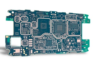
For years, AT&S has worked at the forefront of process and technology development to meet the challenges of continued miniaturization and the demand for better energy efficiency. In this context, the company is involved in various research and development programmes. One current example is the Horizon 2020 EU Research and Innovation programme, in which 11 key European actors are collaborating on the GaNonCMOS project. AT&S is also participating in the Panel-Level Packaging Consortium managed by Fraunhofer IZM.
Optimized energy efficiency with GaN
Over the next four years, the GaNonCMOS project consortium – including AT&S – intends to develop cost‑effective and reliable GaN-based processes, components, modules and integration approaches. In particular, the project aims to exploit the energy-efficiency advantages of GaN (gallium nitride), targeting the production of several demonstrators with GaN power switches and CMOS drivers, as well as new magnetic core materials that will enable switching frequencies up to 200 MHz. Together with optimized embedded PCB technology, the developments should lead to new integrated power components for low-cost, high-reliability systems. Working alongside AT&S on this project are the University of Leuven, Epigan, Fraunhofer, IBM Research, IHP, Tyndall National Institute, PNO Innovation, Recom, NXP Semiconductors and X-FAB Semiconductor.
Advancing miniaturisation with panel-level packaging
The Panel-Level Packaging Consortium has also now been formed. It comprises internationally leading partners such as Intel, ASM Pacific, Hitachi Chemical, AT&S, Evatec, Nanium, Süss MicroTec, Unimicron, Brewer Science, Fujifilm Electronic Materials U.S.A., ShinEtsu, Mitsui Chemicals Tohcello and Semsysco. Together with Fraunhofer IZM as the development hub, the plan is to implement fan-out panel-level packaging (FOPLP), one of the newest packaging trends in microelectronics. FOPLP has a very high miniaturisation potential in both package volume and package density.
During the consortium’s two-year term, known technological elements in wafer-level packaging will be transferred to a large panel format. The technological basis for FOPLP is a reconfigured, moulded panel with embedded components and a thin-film redistribution layer, which together yield an SMD-compatible package. The main advantages of FOPLP are a very thin, substrateless package, low thermal resistance, and good RF characteristics. In addition, passive components such as capacitors, resistors, inductors and antenna structures can be integrated into the redistribution layer. This makes the technology suitable for creating multi-chip packages and System-in-Packages (SiPs).
Based on a panel size of 18″ x 24″ (a PCB manufacturing standard) or even larger sizes, lower packaging costs can be achieved thanks to higher productivity.
Share on:


Testimonial
"We’re proud to call I-Connect007 a trusted partner. Their innovative approach and industry insight made our podcast collaboration a success by connecting us with the right audience and delivering real results."
Julia McCaffrey - NCAB GroupSuggested Items
United Electronics Corporation Unveils Revolutionary CIMS Galaxy 30 Automated Optical Inspection System
09/11/2025 | United Electronics CorporationUnited Electronics Corporation (UEC) today announced the launch of its new groundbreaking CIMS Galaxy 30 Automated Optical Inspection (AOI) machine, setting a new industry standard for precision electronics manufacturing quality control. The Galaxy 30, developed and manufactured by CIMS, represents a significant leap forward in inspection technology, delivering exceptional speed improvements and introducing cutting-edge artificial intelligence capabilities.
Intel Announces Key Leadership Appointments to Accelerate Innovation and Strengthen Execution
09/09/2025 | Intel CorporationIntel Corporation today announced a series of senior leadership appointments that support the company’s strategy to strengthen its core product business, build a trusted foundry, and foster a culture of engineering across the business.
DARPA, State of New Mexico Establish Framework to Advance Quantum Computing
09/08/2025 | DARPAAs part of the Quantum Benchmarking Initiative (QBI), DARPA signed an agreement with the State of New Mexico’s Economic Development Department to create the Quantum Frontier Project.
LPKF Strengthens LIDE Technology Leadership with New Patent Protection in Korea
09/04/2025 | LPKFLPKF Laser & Electronics SE today announced that its groundbreaking LIDE (Laser Induced Deep Etching) technology has received additional patent protection in Korea through the Korean Patent Office (KPCA), effective September 1, 2025.
UHDI Fundamentals: UHDI Technology and Industry 4.0
09/03/2025 | Anaya Vardya, American Standard CircuitsUltra high density interconnect (UHDI) technology is rapidly transforming how smart systems are designed and deployed in the context of Industry 4.0. With its capacity to support highly miniaturized, high-performance, and densely packed electronics, UHDI is a critical enabler of the smart, connected, and automated industrial future. Here, I’ll explore the synergy between UHDI and Industry 4.0 technologies, highlighting applications, benefits, and future directions.