


 The Chemical Connection: Reducing Etch System Water Usage, Part 2
 It’s Only Common Sense: Nice Guys Really Can Finish First
 The Right Approach: I Hear the Train A Comin'
Detecting Mercury with Gold
March 8, 2017 | ACN NewswireEstimated reading time: 1 minute
Mercury is harmful even in small amounts. Detecting it currently requires expensive equipment. Researchers are working on a faster and cheaper alternative: a portable sensor that can perform a rapid analysis in the field. The key is finding something small and accurate enough to do the job.
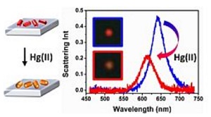
[Left] Amalgam formation on gold nanorods and [Right] scattering color transition (inset) and associated blue shift of the surface plasmon resonance peak wavelengths (λmax) measured in individual nanorods by dark-field microscopy upon chemical reduction of Hg(II). (c)2016 Carola Schopf, Alfonso Martín and Daniela Iacopino.
For many years, scientists have studied tiny gold nanorods for making smaller mercury sensors. Recently, a team from the Tyndall National Institute based at University College Cork found that individual gold nanorods could be used to detect mercury with high sensitivity, making them a strong contender for portable analysers. The results were published in the journal Science and Technology of Advanced Materials.
An individual gold nanorod was fixed to a glass slide that was placed under an electron microscope. Using an imaging method called dark-field microscopy, the team studied the composition of the sample by measuring how light scatters off the rod's surface. A gold nanorod produces a red wavelength pattern, but when it was dipped in a salty solution containing trace levels of mercury, the shape and composition of the rod changed, producing an orange wavelength pattern. The more mercury in the solution, the more the wavelength changed. The nanorods were found to be far more sensitive to mercury than to other metals, including lead, nickel, copper and magnesium.
"The reported linear correlation and high selectivity make this approach potentially suitable for on-site analysis using a miniaturized portable spectrometer," the study concluded.
However, major hurdles remain. The size and shape of gold nanorods vary from rod to rod, significantly throwing off measurements. Manufacturers must improve their fabrication so they are consistent. Also, pre-purification protocols of the rods will be required before real-world analysis can be reliably performed.
Share on:


Suggested Items
The Chemical Connection: Reducing Etch System Water Usage, Part 2
05/02/2024 | Don Ball -- Column: The Chemical ConnectionIn my last column, I reviewed some relatively simple ways to reduce water usage in existing etch systems: cutting down cooling coil water flow, adding chillers to replace plant water for cooling, lowering flow rate nozzles for rinses, etc. This month, I’ll continue with more ways to control water usage in your etcher. Most of these are not easily retrofittable to existing equipment but should be given serious consideration when new equipment is contemplated. With the right combination of add-ons, it is possible to bring the amount of water used in an etch system to almost zero.
Designer’s Notebook: What Designers Need to Know About Manufacturing, Part 2
04/24/2024 | Vern Solberg -- Column: Designer's NotebookThe printed circuit board (PCB) is the primary base element for providing the interconnect platform for mounting and electrically joining electronic components. When assessing PCB design complexity, first consider the component area and board area ratio. If the surface area for the component interface is restricted, it may justify adopting multilayer or multilayer sequential buildup (SBU) PCB fabrication to enable a more efficient sub-surface circuit interconnect.
Insulectro’s 'Storekeepers' Extend Their Welcome to Technology Village at IPC APEX EXPO
04/03/2024 | InsulectroInsulectro, the largest distributor of materials for use in the manufacture of PCBs and printed electronics, welcomes attendees to its TECHNOLOGY VILLAGE during this year’s IPC APEX EXPO at the Anaheim Convention Center, April 9-11, 2024.
ENNOVI Introduces a New Flexible Circuit Production Process for Low Voltage Connectivity in EV Battery Cell Contacting Systems
04/03/2024 | PRNewswireENNOVI, a mobility electrification solutions partner, introduces a more advanced and sustainable way of producing flexible circuits for low voltage signals in electric vehicle (EV) battery cell contacting systems.
Heavy Copper PCBs: Bridging the Gap Between Design and Fabrication, Part 1
04/01/2024 | Yash Sutariya, Saturn Electronics ServicesThey call me Sparky. This is due to my talent for getting shocked by a variety of voltages and because I cannot seem to keep my hands out of power control cabinets. While I do not have the time to throw the knife switch to the off position, that doesn’t stop me from sticking screwdrivers into the fuse boxes. In all honesty, I’m lucky to be alive. Fortunately, I also have a talent for building high-voltage heavy copper circuit boards. Since this is where I spend most of my time, I can guide you through some potential design for manufacturability (DFM) hazards you may encounter with heavy copper design.