


 Fresh PCB Concepts: Key Considerations for Reliability, Performance, and Compliance in PCBs
 Elementary Mr. Watson: Navigating RF—A Glide Path Approach to Design Success
 Designers Notebook: Layer Stackup Planning for RF Circuit Boards


Zuken Partners with Nano Dimension to Develop Seamless Design to Manufacture for 3D Printing
April 5, 2017 | ZukenEstimated reading time: 2 minutes
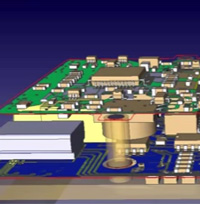
Zuken and Nano Dimension are working together to advance the 3D printing user experience and prototype turnaround times. Nano Dimension, a leader in electronic printing technologies, will take advantage of the support for implementing electronic technologies provided by Zuken’s market-leading, native 3D, system-level design solution, CR-8000 Design Force.
Simon Fried, Chief Business Officer, Nano Dimension, said, “It has been an amazing few years for our company as we’ve fielded interest in our technology. We’re excited about working with Zuken to harness Design Force and take our products even further, giving our users a seamless experience from design to output and optimization.”
Nano Dimension develops advanced 3D printed electronics platforms, including the DragonFly 2020 3D printer for multilayer printed circuit boards, and nanotechnology-based conductive and dielectric inks for their 3D printers. The printer continues to capture global industry and media attention. Future developments will see expansion to support additional board technologies including flexible circuits and embedded components.
Humair Mandavia, Chief Strategy Officer, Zuken USA, said, “Zuken’s CR-8000 Design Force retains all the detailed data needed for 3D printing and allows export direct to manufacturing or 3D printing, without losing integrity. Nano Dimension’s 3D printers are typical of the many applications we envisioned when we pioneered native 3D design for manufacturing.”
Design Force is the sole design tool that allows specification of unique rules for materials, meaning no extra steps are needed when 3D printing to silver and any other future conductive material. Zuken also offers dedicated DFM solutions to support printed electronics via its DFM Inkjet module that optimizes CAD data for inkjet printers. With these solutions from Nano Dimension and Zuken users can expect to spend more time innovating and getting new ideas to market, rather than dealing with design administration.
Movie: Nano Dimension’s DragonFly 2020 3D Printing Platform for Electronics:
About Nano Dimension
Nano Dimension Ltd., founded in 2012, is focused on the research and development of advanced 3D printed electronics, including a 3D printer for multilayer printed circuit boards, and the development of nanotechnology-based conductive and dielectric inks, which are complementary products for 3D printers. Nano Dimension’s novel and proprietary technologies enable the use of conductive and dielectric inks for ultra-rapid prototyping of complex, high-performance multilayer circuit boards. The company’s PCB 3D printer is the result of combining advanced breakthroughs in inkjet technology, 3D printing and nanotechnology.
About Zuken
Zuken is a global provider of leading-edge software and consulting services for electrical and electronic design and manufacturing. Founded in 1976, Zuken has the longest track record of technological innovation and financial stability in the electronic design automation (EDA) software industry. The company’s extensive experience, technological expertise and agility, combine to create world-class software solutions. Zuken’s transparent working practices and integrity in all aspects of business produce long-lasting and successful customer partnerships that make Zuken a reliable long-term business partner.
Zuken is focused on being a long-term innovation and growth partner. The security of choosing Zuken is further reinforced by the company’s people—the foundation of Zuken’s success. Coming from a wide range of industry sectors, specializing in many different disciplines and advanced technologies, Zuken’s people relate to and understand each company’s unique requirements. For more information about the company and its products, visit www.zuken.com.
Share on:


Suggested Items
HyRel Technologies Celebrates Future Innovators: Intern Program Empowers the Next Generation of Engineers and Professionals
05/01/2025 | HyRelHyRel Technologies, a global provider of quick turn semiconductor modification solutions, is proud to spotlight its 7th class of interns in partnership with Peoria Unified School District, featuring three outstanding young women who are already making meaningful contributions to the company's innovative engineering and operations efforts.
SEMI 3D & Systems Summit to Spotlight Trends in Hybrid Bonding, Chiplet Architecture and Geopolitical Dynamics
05/01/2025 | SEMILeading experts in 3D integration and systems for semiconductor manufacturing applications will gather at the annual SEMI 3D & Systems Summit, June 25-27, 2025, in Dresden.
Cadence Expands Design IP Portfolio Optimized for Intel 18A and Intel 18A-P Technologies, Advancing AI, HPC and Mobility Applications
05/01/2025 | Cadence Design SystemsCadence announced a significant expansion of its portfolio of design IP optimized for Intel 18A and Intel 18A-P technologies and certification of Cadence® digital and analog/custom design solutions for the latest Intel 18A process design kit (PDK).
A Visit With ‘Flexperts’ Mark Finstad and Nick Koop
05/01/2025 | Joe Fjelstad, Verdant ElectronicsAt IPC APEX EXPO 2025, I chatted with seasoned flex experts Mark Finstad and Nick Koop about "Flexperts" and their roles as leading educators and in the realm of standards development for this increasingly indispensable electronic interconnection technology. They have been teaching about lessons learned and how to successfully navigate the “seas” of flexible circuits to help their students avoid the hazards that have taken down many of their predecessors in the past.
Siemens Expands Global Electronics Intelligence Reach and Supplyframe Portfolio with Wevolver Acquisition
04/30/2025 | Siemens Digital Industries SoftwareSiemens Digital Industries Software announced its intention to acquire Wevolver, expanding its audience reach, enhancing the Supplyframe product portfolio, and combining digital marketing and integrated campaign programs that include go-to-market support and content creation.