


 The Right Approach: Get Ready for ISO 9001 Version 6
 Dan’s Biz Bookshelf: ‘Still Broke: Walmart’s Remarkable Transformation'
 Driving Innovation: Depth Routing Processes—Achieving Unparalleled Precision in Complex PCBs


AT&S Tech Enables Evaluation of Fully Integrated GaN-based Multilevel Power Converter
April 25, 2017 | AT&SEstimated reading time: 1 minute
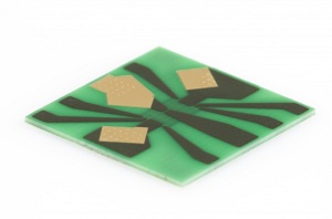
Fraunhofer IAF has developed a fully integrated monolithic multilevel converter in high-volt AlGaN/GaN-on-Si technology. The integrated inverter circuit is designed for maximum voltages of +/- 400 V and currents of 5 A. The multilevel converter on an area of just 2 × 3 mm² comprises four transistors and six diodes. It provides a perfect solution for compact voltage converter applications. It was possible to demonstrate DC/AC inverter operation for American mains voltage. The circuit exhibits minimal dynamic losses at very high frequencies. The excellent switching performance of the multilevel converter was demonstrated with a test setup on the basis of the ECP® technology from AT&S.
A corresponding test setup is necessary in order to evaluate the chip. The packaging of the die constitutes a key factor in this regard. If lateral components are employed, the source, drain and gate pads are on one side and the back of the die is used for heat dissipation. Since the conventional approach with wirebonds imposed restrictions, the second step of the evaluation saw the ECP® technology from AT&S being used. With this technology, the power components – like the multilevel converter – are embedded into the PCB material and can be connected from both sides. The chips are connected directly via copper-plated microvias. This permits low impedance connections and significantly lower inductances compared with wirebond technology. The rear of the die is also connected by means of copper-plated microvias. This ensures excellent heat dissipation.
For more information, click here.
Share on:


Testimonial
"Our marketing partnership with I-Connect007 is already delivering. Just a day after our press release went live, we received a direct inquiry about our updated products!"
Rachael Temple - AlltematedSuggested Items
Closing the Loop on PCB Etching Waste
09/09/2025 | Shawn Stone, IECAs the PCB industry continues its push toward greener, more cost-efficient operations, Sigma Engineering’s Mecer System offers a comprehensive solution to two of the industry’s most persistent pain points: etchant consumption and rinse water waste. Designed as a modular, fully automated platform, the Mecer System regenerates spent copper etchants—both alkaline and acidic—and simultaneously recycles rinse water, transforming a traditionally linear chemical process into a closed-loop system.
Driving Innovation: Depth Routing Processes—Achieving Unparalleled Precision in Complex PCBs
09/08/2025 | Kurt Palmer -- Column: Driving InnovationIn PCB manufacturing, the demand for increasingly complex and miniaturized designs continually pushes the boundaries of traditional fabrication methods, including depth routing. Success in these applications demands not only on robust machinery but also sophisticated control functions. PCB manufacturers rely on advanced machine features and process methodologies to meet their precise depth routing goals. Here, I’ll explore some crucial functions that empower manufacturers to master complex depth routing challenges.
Trouble in Your Tank: Minimizing Small-via Defects for High-reliability PCBs
08/27/2025 | Michael Carano -- Column: Trouble in Your TankTo quote the comedian Stephen Wright, “If at first you don’t succeed, then skydiving is not for you.” That can be the battle cry when you find that only small-diameter vias are exhibiting voids. Why are small holes more prone to voids than larger vias when processed through electroless copper? There are several reasons.
The Government Circuit: Navigating New Trade Headwinds and New Partnerships
08/25/2025 | Chris Mitchell -- Column: The Government CircuitAs global trade winds continue to howl, the electronics manufacturing industry finds itself at a critical juncture. After months of warnings, the U.S. Government has implemented a broad array of tariff increases, with fresh duties hitting copper-based products, semiconductors, and imports from many nations. On the positive side, tentative trade agreements with Europe, China, Japan, and other nations are providing at least some clarity and counterbalance.
How Good Design Enables Sustainable PCBs
08/21/2025 | Gerry Partida, Summit InterconnectSustainability has become a key focus for PCB companies seeking to reduce waste, conserve energy, and optimize resources. While many discussions on sustainability center around materials or energy-efficient processes, PCB design is an often overlooked factor that lies at the heart of manufacturing. Good design practices, especially those based on established IPC standards, play a central role in enabling sustainable PCB production. By ensuring designs are manufacturable and reliable, engineers can significantly reduce the environmental impact of their products.