


 The Chemical Connection: Reducing Etch System Water Usage, Part 2
 It’s Only Common Sense: Nice Guys Really Can Finish First
 The Right Approach: I Hear the Train A Comin'
Unexpected Damage Found Rippling Through Promising Exotic Nanomaterials
April 28, 2017 | BNLEstimated reading time: 4 minutes
Some of the most promising and puzzling phenomena in physics play out on the nanoscale, where a billionth-of-a-meter shift can make or break perfect electrical conductivity.
Now, scientists have developed a new method to probe three-dimensional, atomic-scale intricacies and chemical compositions with unprecedented precision. The breakthrough technique—described February 6 in the journal Nano Letters—combines atomic-force microscopy with near-field spectroscopy to expose the surprising damage wreaked by even the most subtle forces.
“This is like granting sight to the blind,” said lead author Adrian Gozar of Yale University. “We can finally see the all-important variations that dictate functionality at this scale and better explore both cutting-edge electronics and fundamental questions that have persisted for decades.”
Scientists from Yale University, Harvard University, and the U.S. Department of Energy’s Brookhaven National Laboratory developed the technique to determine why a particular device fabrication technique—helium-ion beam lithography—failed to create the scalable, high-performing superconducting nanowires predicted by both theory and simulation.
In previous work, heavy ion beams were used to carve 10-nm-wide channels—some 10,000 times thinner than a human hair—through custom-made materials. However, the new study revealed beam-induced damage rippling out over 50 times that distance. At this scale, that difference was both imperceptible and functionally catastrophic.
“This directly addresses the challenge of quantum computing, for example, where companies including IBM and Google are exploring superconducting nanowires but need reliable synthesis and characterization,” said study coauthor and Brookhaven Lab physicist Ivan Bozovic.
Writing with ions
One promising design for high-temperature superconducting devices is alternating superconductor-insulator-superconductor (SIS) interfaces—or so-called Josephson junctions. These are theoretically easy to fabricate by direct beam writing, assuming sufficient precision can be achieved.
Helium-ion beam lithography (HIB) was a perfect candidate, proven recently in similar materials and well suited for swift and scalable production of superconducting nanowires and Josephson junctions.
“HIB lets us focus the particle beam to less than a single nanometer and effectively ‘write’ patterns to create superconducting interfaces,” said Nicholas Litombe, who led the HIB work under the guidance of Professor Jenny Hoffman of Harvard, a coauthor of this study. “We set out to shift that technique to another class of materials: LSCO thin films.”
The collaboration started with the painstaking assembly of perfect LSCO thin films—so named for their use of lanthanum, strontium, copper, and oxygen. Bozovic’s group at Brookhaven used a technique called atomic layer-by-layer molecular beam epitaxy, which can create atomically perfect superconducting films and heterostructures.
“I have a long-standing interest and specialization in using interphase physics to induce and understand high-temperature superconductivity,” Bozovic said. “HIB gives us an entirely new way to explore these materials on the nanoscale.”
Litombe carved the ultra-precise interface channels in Bozovic’s thin films. But the immediate results were discouraging: the anticipated superconductivity was entirely suppressed when current ran through wires narrower than a couple hundred nanometers.
“Our computer models and experimental results all looked excellent, but we knew there were hidden forces at work,” Litombe said. “We needed deeper insight into the material structure.”
Cryogenic lightning rod
Material composition and electronic properties can be pinpointed through the way they absorb and emit light—a longstanding field called spectroscopy. In the instance of superconductivity, this can distinguish between the “shiny” surface of a conductive metal versus the dullness of a current-breaking insulator.
The scientists turned to scanning near-field optical microscopy (SNOM) to examine the spectroscopic sheen on the HIB pathways. But this technique, which funnels light through a gilded glass capillary, has a resolution limit of about 100 nanometers—much too large to examine the nanoscale superconducting interfaces.
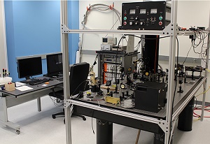
Fortunately, Gozar built a specialized instrument to radically increase the spectroscopic resolution. The machine, built entirely at Brookhaven Lab and now housed at Yale, combines SNOM with atomic force microscopy (AFM). Like a record player’s needle extracting sound from the texture of vinyl, an AFM needle travels over a material and reads the atomic topography.
“Here, the AFM needle acts like a lightning rod, channeling the SNOM light down to just tens of nanometers,” Gozar said. “We have simultaneous AFM topography and spectroscopic data on the deep chemical structures.”
Crucially, Gozar’s AFM-SNOM system also operates at the cryogenic temperatures required to test these materials—a capability only offered at a few laboratories in the world.
Widespread ruin
The novel technique revealed the unexpected and widespread damage left in the wake of the helium ions. Despite the 0.5-nanometer focus of the beam, its effects rattled atoms across a 500-nanometer spread and altered the structure enough to prevent superconductivity. For nanomaterial construction, this so-called lateral straggle is utterly untenable.
“Even the slightest nudge at this scale shatters the powerful phenomena we mean to exploit,” Litombe said. “High-temperature superconductivity can have a coherence distance of just a few atoms, so this lateral effect is devastating. We are, of course, still thrilled to explore the never-before-seen details.”
Added Bozovic, “In one sense, the whole result was negative. Our initial goal of creating nanometer-thick superconducting wires was not fully accomplished. But figuring out why has opened some truly exciting doors.”
The SNOM-AFM technique is readily applicable to fields such as plasmonics for display technology and the study of the mechanism behind high-temperature superconductivity.
“The nanoscale resolution and the tomographic capabilities of the instrument, put us on the cusp of uncovering new truths about nanoscale phenomena and the technology it empowers,” Gozar said.
This research was supported by the U.S. Department of Energy’s Office of Science and the Gordon and Betty Moore Foundation.
Brookhaven National Laboratory is supported by the Office of Science of the U.S. Department of Energy. The Office of Science is the single largest supporter of basic research in the physical sciences in the United States, and is working to address some of the most pressing challenges of our time. For more information, please visit science.energy.gov.
Share on:


Suggested Items
The Chemical Connection: Reducing Etch System Water Usage, Part 2
05/02/2024 | Don Ball -- Column: The Chemical ConnectionIn my last column, I reviewed some relatively simple ways to reduce water usage in existing etch systems: cutting down cooling coil water flow, adding chillers to replace plant water for cooling, lowering flow rate nozzles for rinses, etc. This month, I’ll continue with more ways to control water usage in your etcher. Most of these are not easily retrofittable to existing equipment but should be given serious consideration when new equipment is contemplated. With the right combination of add-ons, it is possible to bring the amount of water used in an etch system to almost zero.
Designer’s Notebook: What Designers Need to Know About Manufacturing, Part 2
04/24/2024 | Vern Solberg -- Column: Designer's NotebookThe printed circuit board (PCB) is the primary base element for providing the interconnect platform for mounting and electrically joining electronic components. When assessing PCB design complexity, first consider the component area and board area ratio. If the surface area for the component interface is restricted, it may justify adopting multilayer or multilayer sequential buildup (SBU) PCB fabrication to enable a more efficient sub-surface circuit interconnect.
Insulectro’s 'Storekeepers' Extend Their Welcome to Technology Village at IPC APEX EXPO
04/03/2024 | InsulectroInsulectro, the largest distributor of materials for use in the manufacture of PCBs and printed electronics, welcomes attendees to its TECHNOLOGY VILLAGE during this year’s IPC APEX EXPO at the Anaheim Convention Center, April 9-11, 2024.
ENNOVI Introduces a New Flexible Circuit Production Process for Low Voltage Connectivity in EV Battery Cell Contacting Systems
04/03/2024 | PRNewswireENNOVI, a mobility electrification solutions partner, introduces a more advanced and sustainable way of producing flexible circuits for low voltage signals in electric vehicle (EV) battery cell contacting systems.
Heavy Copper PCBs: Bridging the Gap Between Design and Fabrication, Part 1
04/01/2024 | Yash Sutariya, Saturn Electronics ServicesThey call me Sparky. This is due to my talent for getting shocked by a variety of voltages and because I cannot seem to keep my hands out of power control cabinets. While I do not have the time to throw the knife switch to the off position, that doesn’t stop me from sticking screwdrivers into the fuse boxes. In all honesty, I’m lucky to be alive. Fortunately, I also have a talent for building high-voltage heavy copper circuit boards. Since this is where I spend most of my time, I can guide you through some potential design for manufacturability (DFM) hazards you may encounter with heavy copper design.