


 The Chemical Connection: Reducing Etch System Water Usage, Part 2
 It’s Only Common Sense: Nice Guys Really Can Finish First
 The Right Approach: I Hear the Train A Comin'
Wafer-thin Magnetic Materials Developed for Future Quantum Technologies
May 22, 2017 | University of BaselEstimated reading time: 2 minutes
Two-dimensional magnetic structures are regarded as a promising material for new types of data storage, since the magnetic properties of individual molecular building blocks can be investigated and modified. For the first time, researchers have now produced a wafer-thin ferrimagnet, in which molecules with different magnetic centers arrange themselves on a gold surface to form a checkerboard pattern. Scientists at the Swiss Nanoscience Institute at the University of Basel and the Paul Scherrer Institute published their findings in the journal Nature Communications.
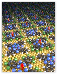
Phthalocyanines with iron (orange) and manganese (violet) centers co-assemble on a gold surface into a checkerboard pattern. The magnetism of iron and manganese differs in strength and points in opposite directions (red and blue arrows), fulfilling the prerequisites for extremely, atomically thin ferrimagnets. (Image: University of Basel, Department of Physics)
Ferrimagnets are composed of two centers which are magnetized at different strengths and point in opposing directions. Two-dimensional, quasi-flat ferrimagnets would be suitable for use as sensors, data storage devices or in a quantum computer, since the two-dimensional arrangement allows the magnification state of the individual atoms or molecules to be selected. For mathematical and geometrical reasons, however, it has so far not been possible to produce two-dimensional ferrimagnets.
Choice of materials makes the impossible possible
The scientists in Professor Thomas Jung’s research groups at the Paul Scherrer Institute (PSI) and the Department of Physics at the University of Basel have now found a method of making a two-dimensional ferrimagnet.
The researchers first produce “phthalocyanines” – hydrocarbon compounds with different magnetic centers composed of iron and manganese. When these phthalocyanines are applied to a gold surface, they arrange themselves into a checkerboard pattern in which molecules with iron and manganese centers alternate. The researchers were able to prove that the surface is magnetic, and that the magnetism of the iron and manganese is of different strengths and appears in opposing directions – all characteristics of a ferrimagnet.
“The decisive factor of this discovery is the electrically conductive gold substrate, which mediates the magnetic order,” explains Dr. Jan Girovsky from the PSI, lead author of the study. “Without the gold substrate, the magnetic atoms would not sense each other and the material would not be magnetic.”
The decisive effect of the conducting electrons in the gold substrate is shown by a physical effect detected in each magnetic atom using scanning tunnel spectroscopy. The experiments were conducted at various temperatures and thus provide evidence of the strength of the magnetic coupling in the new magnetic material. Model calculations confirmed the experimentally observed effect and indicated that special electrons attached to the surface in the gold substrate are responsible for this type of magnetism.
Nanoarchitecture leads to new magnetic materials
“The work shows that a clever combination of materials and a particular nanoarchitecture can be used to produce new materials that otherwise would be impossible,” says Professor Nirmalya Ballav of the Indian Institute of Science Education and Research in Pune (India), who has been studying the properties of molecular nano-checkerboard architectures for several years with Jung. The magnetic molecules have great potential for a number of applications, since their magnetism can be individually investigated and also modified using scanning tunnel spectroscopy.
Original source
Jan Girovsky, Jan Nowakowski, Md. Ehesan Ali, Milos Baljozovic, Harald R. Rossmann, Thomas Nijs, Elise A. Aeby, Sylwia Nowakowska, Dorota Siewert, Gitika Srivastava, Christian Wackerlin, Jan Dreiser, Silvio Decurtins, Shi-Xia Liu, Peter M. Oppeneer, Thomas A. Jung and Nirmalya Ballav
Share on:


Suggested Items
Real Time with… IPC APEX EXPO 2024: Exploring the Future of Surface Finishes
04/25/2024 | Real Time with...IPC APEX EXPOJoe McGurran, product marketing director for MKS Atotech, looks into the future of surface finishes, discussing less nickel, reduced thickness, technologies influencing HDI and UHDI, and the benefits of nickel-free surface finishes. He also touches on popular finishes like ENIG and palladium immersion gold and discusses the value proposition of making a change.
Designer’s Notebook: What Designers Need to Know About Manufacturing, Part 2
04/24/2024 | Vern Solberg -- Column: Designer's NotebookThe printed circuit board (PCB) is the primary base element for providing the interconnect platform for mounting and electrically joining electronic components. When assessing PCB design complexity, first consider the component area and board area ratio. If the surface area for the component interface is restricted, it may justify adopting multilayer or multilayer sequential buildup (SBU) PCB fabrication to enable a more efficient sub-surface circuit interconnect.
IDTechEx Report Unveils 3D Electronics Status and Opportunities
04/22/2024 | PRNewswire3D electronics is an emerging manufacturing approach that enables electronics to be integrated within or onto the surface of objects. 3D electronic manufacturing techniques empower new features, including mass customizability, greater integration, and improved sustainability in the electronics industry.
NASA, Japan Advance Space Cooperation, Sign Agreement for Lunar Rover
04/11/2024 | NASANASA Administrator Bill Nelson and Japan’s Minister of Education, Culture, Sports, Science and Technology (MEXT) Masahito Moriyama have signed an agreement to advance sustainable human exploration of the Moon.
Lockheed Martin Conducts Historic LRASM Flight Test
04/04/2024 | Lockheed MartinThe U.S. Navy in partnership with Lockheed Martin [NYSE: LMT] successfully conducted a historic Long-Range Anti-Ship Missile (LRASM) flight test with four missiles simultaneously in flight.