


 The Chemical Connection: Reducing Etch System Water Usage, Part 2
 It’s Only Common Sense: Nice Guys Really Can Finish First
 The Right Approach: I Hear the Train A Comin'
Let There Be Light: Deterministic Arrays of Quantum Dots
May 22, 2017 | Graphene FlagshipEstimated reading time: 3 minutes
Transition metal dichalcogenides (TMDs) are layered semiconductors that can be exfoliated into layers only a few atoms thick. Recent research has shown that some TMDs can contain quantum light sources that can emit single photons of light. Until now, the occurrence of these quantum light emitters has been random, so they were not suitable for large scale applications. Now, researchers in the Graphene Flagship working at the University of Cambridge, UK, have created large scale arrays of these quantum emitters in different TMD materials. The work, also involving researchers from Harvard University, US, is published in Nature Communications. This new approach leads to large quantities of on-demand, single photon emitters, paving the way for integrating ultra-thin, single photons in electronic devices.
Single photons on demand
Quantum light emitters, or quantum dots, are of interest for many different applications, including quantum communication and networks. Until now, it has been very difficult to produce large arrays of quantum emitters close together while keeping the high quality of the quantum light sources. "It's almost a Goldilocks problem – it seems like one either obtains good single photon sources, or good arrays but not both at the same time. Now, all of a sudden, we can have hundreds of these emitters in one sample," said Mete Atatüre, a professor at the Cavendish Laboratory of the University of Cambridge.
Previous research into quantum emitters in TMDs relied on random occurrences, making systematic production and investigation difficult. "The ability to deterministically create our sources has made a dramatic change in the way we do our day-to-day research. Previously it was pure luck, and we had to keep our spirits high even if we didn't succeed. Now, we can do research in a more systematic way," said Atatüre. Not only does this new method make performing research more straightforward, but it also leads to improvements in the emitters themselves: "The quality of the emitters that we create on purpose seems to be better than the natural quantum dots."
The ability to create deterministic arrays gives a new opportunity to study the TMD quantum emitters in more detail. Dhiren Kara, a researcher at the Cavendish Laboratory, said "There is lots of mystery surrounding these emitters, in how they originate and how they work. Now, one can directly create the emitters and not have to worry about waiting for them to appear randomly. In that sense, it speeds up a lot of the science." Importantly, arrays of quantum emitters were demonstrated in different types of TMD, tungsten diselenide and tungsten disulphide. These materials emit at different wavelengths, which is important for development of future technologies where different types of light are needed. Another avenue the researchers are keen to explore next is the possibility of generating polarised light as stationary qubits for quantum networks, as well as their potential use in optical sensing devices.
The research team at the University of Cambridge. Alejandro R.-P. Montblanch, Andrea Ferrari, Matteo Barbone, Dhiren Kara, Carmen Palacios-Berraquero. Top image: Single photon quantum dots in layered materials semiconductors. Image courtesy Pawel Latawiec/Harvard University.
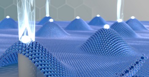
Nanopillars of light
To create the quantum light sources, the researchers cut an array of nanoscale pillars into silica or nanodiamond, and then suspended the few-atom-thick TMD layer on top of the pillars. The quantum emitters are then created in the TMD where it is supported by the pillars, so it is possible to choose exactly where the single photons should be generated. "The fact that the emitters are generated in a mechanical way is good, because it means that they are quite robust, and material independent," said Carmen Palacios-Berraquero, a researcher at the Cavendish Laboratory and first author of the work.
This research is a great step forward to creating on-chip single photon sources. With this deterministic and robust generation of quantum sources, there are new opportunities for hybrid structures of photonic and electronic functions layered together in a single device, and the method is fully scalable and compatible with silicon chip fabrication. "Layered semiconducting materials have distinct unique properties and this realisation of deterministic generation of quantum dots is a real paradigm shift as this has so far been impossible with other materials," said Frank Koppens, of ICFO, Spain, the Leader of the Graphene Flagship Optoelectronics Work Package.
Andrea Ferrari, Science and Technology Officer and Chair of the Management Panel of the Graphene Flagship, was also involved in the research. He added "Quantum technologies are recognized as key investment areas for Europe, with a new Quantum Flagship recently announced. It is great to see that layered materials have now a firm place amongst the promising approaches for generation and manipulation of quantum light and could be enablers of a future integrated technology"
Share on:


Suggested Items
LQDX Divests Aluminum Soldering Business - Mina™ - to Taiyo America Inc.
05/02/2024 | PRNewswireLQDX, formerly known as Averatek Corp., developer of high-performance materials for advanced semiconductor manufacturing, today announced that it has divested its aluminum soldering business – known as MinaTM – to Taiyo America Inc., a global market leader in advanced electronic materials.
Indium Corporation Expert to Present on Pb-Free Solder for Die-Attach in Discrete Power Applications
04/30/2024 | Indium CorporationIndium Corporation Product Manager – Semiconductor Dean Payne will present at the Advanced Packaging for Power Electronics conference, hosted by IMAPS, held May 8-9 in Woburn, Massachusetts, USA.
Real Time with... IPC APEX EXPO 2024: Adhesive Materials and Equipment Update with Dymax
05/01/2024 | Real Time with...IPC APEX EXPOVirginia Hogan, global business development manager at Dymax, discusses adhesive materials, dispensing and curing equipment, a new, high-reliability conformal coating, and various materials and dispensing methods.
Real Time with... IPC APEX EXPO 2024: Sustainability in the Industry
04/26/2024 | Real Time with...IPC APEX EXPOGuest Editor Henry Crandall and Chris Nash of Indium Corporation discuss the company's 90th anniversary and its focus on sustainability. They focus on the benefits of sustainable materials, their compatibility, and value propositions. The conversation also highlights how Durafuse LT technology's role in reducing reflow temperatures is leading to significant cost and energy savings. Nash also touches on downstream sustainability efforts such as using recycled materials for packaging.
SMC Korea 2024 to Highlight Semiconductor Materials Trends and Innovations on Industry’s Path to $1 Trillion
04/24/2024 | SEMIWith Korea a major consumer of semiconductor materials and advanced materials a key driver of innovation on the industry’s path to $1 trillion, industry leaders and experts will gather at SMC (Strategic Materials Conference) Korea 2024 on May 29 at the Suwon Convention Center in Gyeonggi-do, South Korea to provide insights into the latest materials developments and trends. Registration is open.