


 The Chemical Connection: Reducing Etch System Water Usage, Part 2
 It’s Only Common Sense: Nice Guys Really Can Finish First
 The Right Approach: I Hear the Train A Comin'
Unexpected Property May Raise Material’s Prospects as Solar Cell
May 23, 2017 | NISTEstimated reading time: 4 minutes
Crystalline materials known as perovskites could become the next superstars of solar cells. Over the past few years, researchers have demonstrated that a special class of perovskites—those consisting of a hybrid of organic and inorganic components—convert sunlight into electricity with an efficiency above 20 percent and are easier to fabricate and more impervious to defects than the standard solar cell made of crystalline silicon. As fabricated today, however, these organic/inorganic perovskites (OIPs) deteriorate well before the typical 30-year lifetime for silicon cells, which prevents their widespread use in harnessing solar power.
Now a team led by Andrea Centrone at the National Institute of Standards and Technology (NIST) and Jinsong Huang and Alexei Gruverman of the University of Nebraska has found the first solid evidence for a property of OIPs that may provide a new way to improve their long-term stability as solar cells.
The unexpected feature that the team found is known as ferroelasticity—a spontaneous rearrangement of the internal structure of OIPs in which each crystal subdivides into a series of tiny regions, or domains, that have the same atomic arrangement but which are oriented in different directions. This rearrangement creates a spontaneous strain in each domain that exists even in the absence of any external stress (force).
“The role of the ferroelastic domains on the material stability must be understood,” said Centrone.
At high temperatures, OIP crystals do not subdivide and have the same cubic arrangement of atoms throughout. At room temperature, however, the OIP crystal structure changes from cubic to tetragonal, in which one axis of the cube elongates. That’s where the ferroelastic property of the material comes into play.
“To transform from a cubic to a tetragonal arrangement, one axis of the cube must elongate. In the process, each crystal subdivides into smaller domains in which the elongated axis can point in a different direction, leading to spontaneous internal strain,” explained team member Evgheni Strelcov of NIST and the University of Maryland.
At present, it remains unknown whether ferroelasticity is a property that improves or hinders the performance and stability of perovskite solar cells, noted Centrone. But the very fact that OIPs have this internal structure, breaking up single crystals into domains, is important to investigate, he added. Boundaries between crystals—so-called inter-grain boundaries—are known to be weak points, where structural defects concentrate. Similarly, the boundaries between the newly discovered ferroelastic domains inside a single crystal—intra-grain boundaries—might also affect the stability of OIPs and their performance as solar cells.
Image recorded by an atomic force microscope reveals the topography of a polycrystalline sample of the perovskite, including the boundaries between crystals. Credit: NIST
Image taken with the photothermal induced resonance technique shows the newly discovered ferroelastic domains (striations) within most crystals. Scale shows the PTIR signal intensity, a measure of the infrared light absorbed by the sample. Credit: NIST
The researchers discovered that by bending the crystals, they could reliably move, create or eliminate the ferroelastic grain boundaries—the borders between subdivided crystal regions having different orientations—thus enlarging or reducing the size of each domain. The bending also changed the relative fraction of domains pointing in different orientations. The researchers recently described their work (link is external) in Science Advances.
In their study, the team found no evidence that the OIPs were ferroelectric; in other words, that they formed domains where the separation of the center of positive and negative electric charges is aligned in different directions in the absence of an external electric field. This finding is significant, because some researchers had speculated that ferroelectricity might be the underlying property that makes OIPs promising candidates for solar cells.
The researchers created single whole crystals large enough to reveal ferroelastic domains, which appeared as striations with an optical microscope. They also studied OIPs consisting of polycrystalline thin films, which were examined using nanoscale techniques.
The researchers used two nanoscale methods employing atomic force microscope (AFM) probes to measure ferroelasticity in OIP thin films. At the University of Nebraska, Gruverman and his collaborators used piezoresponse force microscopy (PFM), which mapped the electrically induced mechanical response of an OIP sample in repose and under mechanical stress by gently bending the sample.
Illustration shows that in response to an applied stress, such as bending, the boundaries of the ferroelastic domains (red and blue regions depict domains oriented in different directions) become bigger or smaller. Credit: NIST
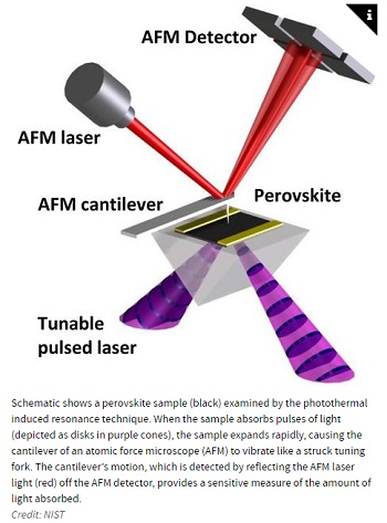
In the other method, laser pulses spanning from the visible to the infrared ranges struck a perovskite thin film, causing the material to heat up and expand. The tiny expansion was captured and amplified by the AFM probe using photothermal induced resonance (PTIR), a technique that combines the resolution of an AFM with the precise compositional information provided by infrared spectroscopy. PTIR imaging revealed the presence of microscopic striations that persisted even when the samples were subjected to heating or applied voltage. Experiments showed that the striations were not correlated with the local chemical composition or optical properties, but were due to differences in thermal expansion coefficient of the ferroelastic domains.
Share on:


Suggested Items
Real Time with… IPC APEX EXPO 2024: Direct Imaging Equipment and Quad-wave DLP Light Engine Technology
05/03/2024 | Real Time with...IPC APEX EXPOGuest Editor Kelly Dack and MivaTek's Brendan Hogan delve into the company's innovative technologies, including direct imaging equipment and quad-wave DLP light engine technology. They highlight the benefits of direct imaging, compensation, and DART technology.
Merlin Flex invests in New Schmoll Direct Imaging System
04/30/2024 | Merlin Flex LtdMerlin Flex has fully installed and commissioned its 2nd Schmoll MDI Direct Imaging system. This new machine includes a twin bed, 4 head system which enhances Merlin Flex’s direct imaging capability for its 1.4M long flexible circuits.
Inkjet Solder Mask ‘Has Arrived’
04/10/2024 | Pete Starkey, I-Connect007I was delighted to be invited to attend an interactive webinar entitled “Solder Mask Coating Made Easy with Additive Manufacturing,” hosted by SUSS MicroTec Netherlands in Eindhoven. The webinar was introduced and moderated by André Bodegom, managing director at Adeon Technologies, and the speakers were Mariana Van Dam, senior product manager PCB imaging solutions at AGFA in Belgium; Ashley Steers, sales manager at Electra Polymers in the UK; and Dr. Luca Gautero, product manager at SUSS MicroTec Netherlands.
NetVia Group Acquires Direct Imaging from Mivatek
04/09/2024 | Miva TechnologiesMiva Technologies is pleased to announce NetVia Group, Irving, TX has acquired a new Miva 2400NG Dual Tray Direct Imaging System with 30-micron capabilities for inner, outer and soldermask imaging.
Teledyne to Acquire Adimec
02/13/2024 | TeledyneTeledyne Technologies Incorporated announced that it has entered into an agreement to acquire Adimec Holding B.V. and its subsidiaries.