


 The Chemical Connection: Reducing Etch System Water Usage, Part 2
 It’s Only Common Sense: Nice Guys Really Can Finish First
 The Right Approach: I Hear the Train A Comin'
Making Wires of Polymer Chains
June 16, 2017 | A*STAREstimated reading time: 2 minutes
Consumer demand continually pushes the electronics industry to design smaller devices. Now researchers at A*STAR have used a theoretical model to assess the potential of electric wires made from polymer chains that could help with miniaturization.
As conventional silicon-integrated circuits reach their lower size limit, new concepts are required such as molecular electronics — the use of electronic components comprised of molecular building blocks. Shuo-Wang Yang at A*STAR Institute of High Performance Computing together with his colleagues and collaborators, are using computer modeling to design electric wires made of polymer chains.
“It has been a long-standing goal to make conductive molecular wires on traditional semiconductor or insulator substrates to satisfy the ongoing demand miniaturization in electronic devices,” explains Yang.
Progress has been delayed in identifying molecules that both conduct electricity and bind to substrates. “Structures with functional groups that facilitate strong surface adsorption typically exhibit poor electrical conductivity, because charge carriers tend to localize at these groups,” he adds.
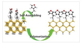
Yang’s team applied density functional theory to a two-step approach for synthesizing linear polymer chains on a silicon surface1,2. “This theory is the best simulation method for uncovering the mechanism behind chemical reactions at atomic and electronic levels. It can be used to predict the reaction pathways to guide researchers,” says Yang.
The first step is the self-assembled growth of single monomers on to the silicon surface. Yang’s team studied several potential monomers including, most recently, a thiophene substituted alkene1 and a symmetrical benzene ring with three alkynes attached2. The second step is the polymerization of the tethered monomers by adding a radical to the system.
According to the calculations, these tethered polymers are semiconductors in their natural state. “We introduced some holes, such as atomic defects, to the wires to shift the Fermi levels and make them conductive,” Yang explains.
The team then studied the electron band structures of each component before and after tethering and polymerization; finding little charge transfer between the molecular wires and the silicon surfaces. “The surface-grafted polymers and underlying substrates seem independent of each other, which is an ideal model of a conductive molecular wire on a traditional semiconductor substrate,” says Yang.
“Our finding provides a theoretical guide to fabricating ideal molecular wires on traditional semiconducting surfaces,” he adds. The team is plans to extend their work to study 2D analogs of these 1D polymer chains that could work as a metallic layer in molecular electronic devices.
Share on:


Suggested Items
Real Time with… IPC APEX EXPO 2024: Exploring the Future of Surface Finishes
04/25/2024 | Real Time with...IPC APEX EXPOJoe McGurran, product marketing director for MKS Atotech, looks into the future of surface finishes, discussing less nickel, reduced thickness, technologies influencing HDI and UHDI, and the benefits of nickel-free surface finishes. He also touches on popular finishes like ENIG and palladium immersion gold and discusses the value proposition of making a change.
Designer’s Notebook: What Designers Need to Know About Manufacturing, Part 2
04/24/2024 | Vern Solberg -- Column: Designer's NotebookThe printed circuit board (PCB) is the primary base element for providing the interconnect platform for mounting and electrically joining electronic components. When assessing PCB design complexity, first consider the component area and board area ratio. If the surface area for the component interface is restricted, it may justify adopting multilayer or multilayer sequential buildup (SBU) PCB fabrication to enable a more efficient sub-surface circuit interconnect.
IDTechEx Report Unveils 3D Electronics Status and Opportunities
04/22/2024 | PRNewswire3D electronics is an emerging manufacturing approach that enables electronics to be integrated within or onto the surface of objects. 3D electronic manufacturing techniques empower new features, including mass customizability, greater integration, and improved sustainability in the electronics industry.
NASA, Japan Advance Space Cooperation, Sign Agreement for Lunar Rover
04/11/2024 | NASANASA Administrator Bill Nelson and Japan’s Minister of Education, Culture, Sports, Science and Technology (MEXT) Masahito Moriyama have signed an agreement to advance sustainable human exploration of the Moon.
Lockheed Martin Conducts Historic LRASM Flight Test
04/04/2024 | Lockheed MartinThe U.S. Navy in partnership with Lockheed Martin [NYSE: LMT] successfully conducted a historic Long-Range Anti-Ship Missile (LRASM) flight test with four missiles simultaneously in flight.