


 Happy’s Tech Talk #28: The Power Mesh Architecture for PCBs
 It’s Only Common Sense: Would You Join Your Own Company?
 The Chemical Connection: Reducing Etch System Water Usage, Part 2
Hands off Approach to Looking Into Silicon Chips
June 29, 2017 | London Centre for NanotechnologyEstimated reading time: 2 minutes
The possibility of looking inside silicon chips to see their tiny working parts, without damaging the chips, is a step closer thanks to an international team led by scientists at the LCN.
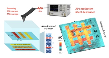
Figure: Microwave Microscope visualizes 3D structures of atomically thin phosphorus layers buried 5-15 nm below a silicon surface
The group at the LCN, led by Dr Neil Curson, have shown that they can generate pictures of tiny three-dimensional components made from phosphorus atoms, that are completely invisible to all other imaging technologies.
Remarkably, the pictures of these components were obtained despite the fact that the components were the size of only a few tens of atoms, were atomically thin and were buried under the surface of the chip. An accurate quantitative determination of the location of the buried components was obtained, along with certain electrical properties. This breakthrough is published in Science Advances.
The components that were studied, including a three-dimensional criss-cross of metallic phosphorus stripes, were designed and manufactured by LCN PhD student Alex Kölker. He used a super-sharp metal needle to write patterns in a single layer of hydrogen atoms that lay on the surface of a silicon chip, creating a template of a desired shape. By causing a chemical reaction to happen between the surface of the chip and phosphine gas, phosphorus atoms were written into the surface, in the shape of the template. The phosphorus structures were then buried with more silicon to complete the device.
A recently developed scanning microwave microscope was used to take pictures of the components, obtained with our collaborators at Johannes Kepler University, led by Georg Gramse, and by Keysight Technologies (Austria), Paul Scherrer Institut, ETH Zürich and EPF Lausanne (Switzerland). The microscope works by focussing microwaves (like those from a microwave oven), to the end of a metal tip which is pushed against the surface of the chip. The microwaves are fired into chip, subsequently bouncing back from the buried components, measured, and used to construct a picture.
According to Dr Curson “The work is potentially of global significance because silicon chips are becoming so sophisticated and intricate that taking snapshots of their smallest working parts is incredibly difficult and time consuming, and currently involves destroying the chip. If we could easily see all components of a chip, in a non-destructive manor, it would be a game-changer. What we have done is a big step towards just that. Such technologies are also becoming important for governments who are interested in knowing what is inside the foreign electronics they are using!”
“Another important application of our imaging technology is in assisting in the fabrication of phosphorus-in-silicon quantum computers, which have the potential to revolutionise computing completely, if realised.”
Dr Ferry Kienberger from Keysight Technologies says “Our company sees this work as a major breakthrough in demonstrating that scanning microwave microscopy is the way forward for the characterisation of the next generation of electrical devices and quantum components in silicon.”
The capabilities demonstrated here are transformative for non-invasive diagnostics of atomic-scale electric components that will form the next generation of “classical” and quantum devices.
Share on:


Suggested Items
Micross, Sital Announce Global Manufacturing & Distribution Partnership
05/07/2024 | Micross Components, Inc.Micross Components, Inc., a leading global provider of mission-critical microelectronic components and services for high-reliability aerospace, defense, space and industrial applications, is pleased to announce our exclusive partnership with Sital Technology (sitaltech.com), the leader in MIL-STD-1553 IP cores, specializing in integrated FPGA solutions.
AT&S Brings High-Tech to the Museumsquartier
05/06/2024 | AT&SAT&S, as a “MQ goes Green” partner, has prepared special highlights for the occasion: Visitors aged eight and above can embark on an interactive journey through the fascinating world of microelectronics.
Argonne, Toyota Collaborate on Cutting-Edge Battery Recycling Process
05/01/2024 | BUSINESS WIREThe U.S. Department of Energy’s (DOE) Argonne National Laboratory has recently launched a collaboration with Toyota Motor North America that could reduce the nation’s reliance on foreign sources of battery materials.
Europlacer Presents New Range of iineo SMT Placement Machines.
05/01/2024 | EuroplacerFor more than 15 years, the Europlacer iineo placement machines have made their mark on the SMT industry with unique features and unrivalled flexibility. Today, Europlacer announces the launch of the second generation iineo.
IPC's Vision for Empowering PCB Design Engineers
04/30/2024 | Robert Erickson, IPCAs architects of innovation, printed circuit board designers are tasked with translating increasingly complex concepts into tangible designs that power our modern world. IPC provides the necessary community, standards framework, and education to prepare these pioneers as they explore the boundaries of what’s possible, equipping engineers with the knowledge, skills, and resources required to thrive in an increasingly dynamic field.