


 It’s Only Common Sense: Nice Guys Really Can Finish First
 The Right Approach: I Hear the Train A Comin'
 Marcy's Musings: The Growing Industry
Taking Technology to the Next Level
July 28, 2017 | CUDOSEstimated reading time: 3 minutes
Physicists from the ARC Centre of Excellence for Ultrahigh bandwidth Devices for Optical Systems (CUDOS) developed a new hybrid integrated platform that promises to be a more advanced alternative to conventional integrated circuits that are currently manufactured by the semiconductor industry. The researchers demonstrated that their approach is mass manufacturable, making it possible to integrate the platform into everyday electronic equipment like smartphones and computers. For the end user this technical advance means that it may lead to faster internet on their next-generation electronic devices.
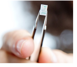
The new device is smaller than a thumbnail with a size of 0.1 x 4mm, and could be integrated into everyday electronic devices like smartphones.
Integrated circuits, so called ‘chips’, are used in everyday electronic equipment like mobile phones and computers. It is a set of electronic circuits on one small flat piece of semiconductor material, normally silicon. But this material has some limitations when it comes to processing data. To overcome these limitations and improve data processing, researchers are developing optical circuits made of chalcogenide glass. This special type of glass is used for ultrafast telecommunication networks, transferring information at the speed of light. Integrating these glass optical circuits into silicon chips could lead to a more advanced communications system, processing data a hundred times faster. Can these two materials be combined?
The answer is yes! In a collaboration with physicists in the University of Sydney’s Australian Institute for Nanoscale Science and Technology (AINST), the Australian National University (ANU) and RMIT University, the CUDOS research group around PhD candidate Blair Morrison and senior researcher Dr Alvaro Casas Bedoya created compact, mass manufacturable optical circuits with enhanced functionalities by combining nonlinear glasses with silicon-based material.
“In the last few years the group at the University of Sydney has repeatedly demonstrated exciting functionalities, such as broadband microwave devices that can enhance radar, using these novel chalcogenide glasses,” Blair Morrison said from the University of Sydney CUDOS node.
“Now we have shown it is possible to combine this material with the current industry standard platform for photonic integration, silicon,” he said.
“We integrated a novel nonlinear glass into an industrially scalable CMOS compatible platform. We maintained the key advantages of both the silicon and the glass, and made a functional and efficient ultra-compact optical circuit,” said Dr Alvaro Casas Bedoya who is the lead photonics nanofabrication manager for CUDOS.
“A wealth of new opportunities will be created, and this takes us one step closer to moving our research from the lab into industrial applications,” said Blair Morrison.
CUDOS Director and ARC Laureate Fellow Professor Benjamin Eggleton from the University of Sydney said this new approach will one day allow the industry to miniaturise the photonics functionalities from devices that are the size of a laptop to the size of a smartphone and even smaller, allowing for deployment in real world applications.
“This is exciting, because this is a platform which is more compatible with existing semiconductor manufacturing and will allow us to integrate multiple functionalities on a single silicon chip, with active and passive components, such as detectors and modulators, required for advanced applications,” said Professor Eggleton who supervised the project.
The multi-university research team went through the whole manufacturing process: The fabrication of these devices uses silicon wafers from a semiconductor foundry in Belgium, a dedicated facility in ANU’s Laser Physics Centre for the glass deposition, lithography in the RMIT University’s School of Engineering and are then characterised and tested in the University of Sydney’s AINST.
To showcase the potential of the new approach, the CUDOS researchers further demonstrated a compact novel laser based on the light-sound interactions, the first time in an integrated optical circuit.
“The breakthrough here is this realisation that we can actually interface, we can integrate that glass onto silicon and we can interface from silicon to the glass very efficiently – we can harness the best of both worlds,” Professor Eggleton said.
Professor Susan Pond, the Director of AINST, emphasized that this project is one of AINST flagship activities that deals with harnessing interactions between photons and phonon at the nanoscale. This work links fundamental research in light matter interactions at the nanoscale with an end user perspective and strong coupling to industry.
Share on:


Suggested Items
ZESTRON Academy Launches 2024 Advanced Packaging & Power Electronics Webinar Series
05/01/2024 | ZESTRONZESTRON, the leading global provider of high-precision cleaning products, services, and training solutions in the electronics manufacturing and semiconductor industries, proudly announces the launch of its highly anticipated webinar series on Advanced Packaging & Power Electronics, a webinar series on the latest innovations, cleaning, and corrosion challenges.
Worldwide Silicon Wafer Shipments Dip 5% in Q1 2024
05/01/2024 | SEMIWorldwide silicon wafer shipments decreased 5.4% quarter-over-quarter to 2,834 million square inches in the first quarter of 2024, a 13.2% drop from the 3,265 million square inches recorded during the same quarter last year, the SEMI Silicon Manufacturers Group (SMG) reported in its quarterly analysis of the silicon wafer industry.
NextFlex Convenes the Hybrid Electronics Community at Binghamton University
05/01/2024 | NextFlexBinghamton University hosted the NextFlex hybrid electronics community on April 18 for a day of expert presentations, breakout sessions on technology and manufacturing topics, and networking.
HQ NextPCB of HQ Electronics Debut on the International Stage for Electronics Manufacture at IPC APEX 2024
05/01/2024 | PRNewswireHQ NextPCB of HQ Electronics, a leading Chinese-based multilayer PCB manufacturer and assembly house showcased its industrial prowess on the international stage for the first time at the IPC APEX Expo 2024.
GPV’s Q1 2024 Interim Financial Report Shows Strong Navigation in Uncertain Times
05/01/2024 | GPVDanish-based GPV recorded an expected drop in sales to DKK 2.3 billion for the first quarter of 2024. The decline also affected the operating profit, which was DKK 155 million compared to DKK 179 million in the same quarter last year, although the EBITDA margin was maintained. In general, demand has been softer in 2024, but GPV continues to invest for the long-term and expects the trend to turn in the second half of 2024.