


 The Chemical Connection: Reducing Etch System Water Usage, Part 2
 It’s Only Common Sense: Nice Guys Really Can Finish First
 The Right Approach: I Hear the Train A Comin'
New Method to Detect Spin Current in Quantum Materials Unlocks Potential for Alternative Electronics
October 16, 2017 | ORNLEstimated reading time: 3 minutes
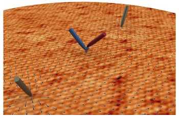
A new method that precisely measures the mysterious behavior and magnetic properties of electrons flowing across the surface of quantum materials could open a path to next-generation electronics.
Found at the heart of electronic devices, silicon-based semiconductors rely on the controlled electrical current responsible for powering electronics. These semiconductors can only access the electrons’ charge for energy, but electrons do more than carry a charge. They also have intrinsic angular momentum known as spin, which is a feature of quantum materials that, while elusive, can be manipulated to enhance electronic devices.
A team of scientists, led by An-Ping Li at the Department of Energy’s Oak Ridge National Laboratory, has developed an innovative microscopy technique to detect the spin of electrons in topological insulators, a new kind of quantum material that could be used in applications such as spintronics and quantum computing.
“The spin current, namely the total angular momentum of moving electrons, is a behavior in topological insulators that could not be accounted for until a spin-sensitive method was developed,” Li said.
Electronic devices continue to evolve rapidly and require more power packed into smaller components. This prompts the need for less costly, energy-efficient alternatives to charge-based electronics. A topological insulator carries electrical current along its surface, while deeper within the bulk material, it acts as an insulator. Electrons flowing across the material’s surface exhibit uniform spin directions, unlike in a semiconductor where electrons spin in varying directions.
“Charge-based devices are less energy efficient than spin-based ones,” said Li. “For spins to be useful, we need to control both their flow and orientation.”
To detect and better understand this quirky particle behavior, the team needed a method sensitive to the spin of moving electrons. Their new microscopy approach was tested on a single crystal of Bi2Te2Se, a material containing bismuth, tellurium and selenium. It measured how much voltage was produced along the material’s surface as the flow of electrons moved between specific points while sensing the voltage for each electron’s spin.
The new method builds on a four-probe scanning tunneling microscope—an instrument that can pinpoint a material’s atomic activity with four movable probing tips—by adding a component to observe the spin behavior of electrons on the material’s surface. This approach not only includes spin sensitivity measurements. It also confines the current to a small area on the surface, which helps to keep electrons from escaping beneath the surface, providing high-resolution results.
“We successfully detected a voltage generated by the electron’s spin current,” said Li, who coauthored a paper published by Physical Review Letters that explains the method. “This work provides clear evidence of the spin current in topological insulators and opens a new avenue to study other quantum materials that could ultimately be applied in next-generation electronic devices.”
Additional coauthors of the study titled, “Detection of the Spin-Chemical Potential in Topological Insulators Using Spin-Polarized Four-Probe STM,” include ORNL’s Saban Hus, Giang Nguyen, Wonhee Ko and Arthur Baddorf; X.-G. Zhang of the University of Florida; and Yong Chen of Purdue University.
This research was conducted at the Center for Nanophase Materials Sciences, a DOE Office of Science User Facility. The development of the novel microscopy method was funded by ORNL’s Laboratory Directed Research and Development program.
ORNL is managed by UT-Battelle for DOE’s Office of Science. The Office of Science is the single largest supporter of basic research in the physical sciences in the United States, and is working to address some of the most pressing challenges of our time. For more information, please click here.
Share on:


Suggested Items
LQDX Divests Aluminum Soldering Business - Mina™ - to Taiyo America Inc.
05/02/2024 | PRNewswireLQDX, formerly known as Averatek Corp., developer of high-performance materials for advanced semiconductor manufacturing, today announced that it has divested its aluminum soldering business – known as MinaTM – to Taiyo America Inc., a global market leader in advanced electronic materials.
Indium Corporation Expert to Present on Pb-Free Solder for Die-Attach in Discrete Power Applications
04/30/2024 | Indium CorporationIndium Corporation Product Manager – Semiconductor Dean Payne will present at the Advanced Packaging for Power Electronics conference, hosted by IMAPS, held May 8-9 in Woburn, Massachusetts, USA.
Real Time with... IPC APEX EXPO 2024: Adhesive Materials and Equipment Update with Dymax
05/01/2024 | Real Time with...IPC APEX EXPOVirginia Hogan, global business development manager at Dymax, discusses adhesive materials, dispensing and curing equipment, a new, high-reliability conformal coating, and various materials and dispensing methods.
Real Time with... IPC APEX EXPO 2024: Sustainability in the Industry
04/26/2024 | Real Time with...IPC APEX EXPOGuest Editor Henry Crandall and Chris Nash of Indium Corporation discuss the company's 90th anniversary and its focus on sustainability. They focus on the benefits of sustainable materials, their compatibility, and value propositions. The conversation also highlights how Durafuse LT technology's role in reducing reflow temperatures is leading to significant cost and energy savings. Nash also touches on downstream sustainability efforts such as using recycled materials for packaging.
SMC Korea 2024 to Highlight Semiconductor Materials Trends and Innovations on Industry’s Path to $1 Trillion
04/24/2024 | SEMIWith Korea a major consumer of semiconductor materials and advanced materials a key driver of innovation on the industry’s path to $1 trillion, industry leaders and experts will gather at SMC (Strategic Materials Conference) Korea 2024 on May 29 at the Suwon Convention Center in Gyeonggi-do, South Korea to provide insights into the latest materials developments and trends. Registration is open.