


 It’s Only Common Sense: Nice Guys Really Can Finish First
 The Right Approach: I Hear the Train A Comin'
 Marcy's Musings: The Growing Industry
View the Chemical Reactions of Nanostructures Live
November 3, 2017 | DTUEstimated reading time: 2 minutes
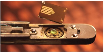
DTU Nanotech has developed microchip based systems that enable imaging on the molecular scale of processes in liquids. Used in connection with scanning or transmission electron microscopes (SEM and TEM), it allows you to reveal the intricate details of reactions at interfaces between particles, solid surfaces and liquids, such as e.g. corrosion or crystallisation processes.
Nanostructured solid-liquid interfaces are present everywhere in daily life, in products and production. The structures change during production, use, or aging. Optical microscopy or x-ray methods have traditionally been the main methods to image what is taking place in processes at the solid-liquid interface, but these are very limited in their resolution compared to the often complex processes actually taking place on the nanoscale.
“It is comparable to a crime scene investigation in which the case description by the detective trying to deduce what took place has far less information and details than is apparent to the direct observer. Many processes are well understood in their macroscopic ‘average’ behaviour, while obtaining detailed microscopic knowledge could provide new understandings and opportunities in a wide variety of applications, such as corrosion, scaling, nucleation and precipitation of materials, and electrochemical processes such as plating, electrocatalysis or energy conversion processes in batteries and fuel cells,” says group leader Kristian Mølhave.
Transmission electron microscopy of a liquid chemical reaction. Gold ions react with silver nanostructures to deposit gold on the surface while etching the internal silver nanostructure to form a gold nano-cage in a galvanic replacement reaction.
Detailed images of complex processes
PhD student Murat Nulati Yesibolati has built and refined systems for both SEM and TEM, where microchips with 50 nanometer thick membranes form electron transparent windows that allow us to follow liquid phase processes on microelectrodes and microscale heaters, with electron microscope resolution. Yesibolati explains: “The systems rely on a common microchip layout that makes it possible easily to shift between them and also provides more capabilities than the commercially available systems today”.
Another PhD student, Simone Lagana, has created an alternative system that has better control over the liquid layer thickness and hence an image resolution. This is based on suspended nanochannels in ultrathin silicon nitride films which provide a more self-contained single-use disposable unit that could be used more easily in other laboratories.
“With these systems we are able to get completely new detailed images of complex processes, and also begin to use advanced electron microscopy methods such as electron holography that can provide entirely new information about electric and magnetic fields in the systems” says Murat Nulati Yesibolati who is working on this.
The group has been using the platform to study the details of dendritic growth with copper as a model system. The dendrite growth process is an intricate interplay of the electrical fields at the structurally evolving electrode surface and how it influences the supply of copper ions from the electrolyte. These observations are used to test finite element model simulations of the process conducted at DTU Physics by Professor Henrik Bruus who says “this level of resolution and quantitative comparison of our calculations has never been possible before!”
“Based on these new capabilities to perform real time quantitative measurements of the reaction dynamics in such a range of fundamental reactions, we are pushing towards using the liquid cell platforms to study ever more real-world relevant chemical processes. We are of course very interested in collaborating with people who have a nanoscale reaction where these new exciting possibilities can help them get a better understanding to optimise their processes and products!” says Kristian Mølhave.
Share on:


Suggested Items
Designer’s Notebook: What Designers Need to Know About Manufacturing, Part 2
04/24/2024 | Vern Solberg -- Column: Designer's NotebookThe printed circuit board (PCB) is the primary base element for providing the interconnect platform for mounting and electrically joining electronic components. When assessing PCB design complexity, first consider the component area and board area ratio. If the surface area for the component interface is restricted, it may justify adopting multilayer or multilayer sequential buildup (SBU) PCB fabrication to enable a more efficient sub-surface circuit interconnect.
Insulectro’s 'Storekeepers' Extend Their Welcome to Technology Village at IPC APEX EXPO
04/03/2024 | InsulectroInsulectro, the largest distributor of materials for use in the manufacture of PCBs and printed electronics, welcomes attendees to its TECHNOLOGY VILLAGE during this year’s IPC APEX EXPO at the Anaheim Convention Center, April 9-11, 2024.
ENNOVI Introduces a New Flexible Circuit Production Process for Low Voltage Connectivity in EV Battery Cell Contacting Systems
04/03/2024 | PRNewswireENNOVI, a mobility electrification solutions partner, introduces a more advanced and sustainable way of producing flexible circuits for low voltage signals in electric vehicle (EV) battery cell contacting systems.
Heavy Copper PCBs: Bridging the Gap Between Design and Fabrication, Part 1
04/01/2024 | Yash Sutariya, Saturn Electronics ServicesThey call me Sparky. This is due to my talent for getting shocked by a variety of voltages and because I cannot seem to keep my hands out of power control cabinets. While I do not have the time to throw the knife switch to the off position, that doesn’t stop me from sticking screwdrivers into the fuse boxes. In all honesty, I’m lucky to be alive. Fortunately, I also have a talent for building high-voltage heavy copper circuit boards. Since this is where I spend most of my time, I can guide you through some potential design for manufacturability (DFM) hazards you may encounter with heavy copper design.
Trouble in Your Tank: Supporting IC Substrates and Advanced Packaging, Part 5
03/19/2024 | Michael Carano -- Column: Trouble in Your TankDirect metallization systems based on conductive graphite or carbon dispersion are quickly gaining acceptance worldwide. Indeed, the environmental and productivity gains one can achieve with these processes are outstanding. In today’s highly competitive and litigious environment, direct metallization reduces costs associated with compliance, waste treatment, and legal issues related to chemical exposure. What makes these processes leaders in the direct metallization space?