


 The Chemical Connection: Reducing Etch System Water Usage, Part 2
 It’s Only Common Sense: Nice Guys Really Can Finish First
 The Right Approach: I Hear the Train A Comin'
Carbon Atoms Assemble Themselves on Command
November 7, 2017 | DTUEstimated reading time: 3 minutes
Using a new method that gets carbon atoms to assemble themselves, researchers open up for opportunities to create quantum dots that can revolutionize the information technology of the future.
To enable computers and storage media to keep up with the skyrocketing volumes of data that need to be stored and processed, researchers and companies are investing huge sums in lithographic processes that can create ultra-small patterns for the electronic components on which the information society is based. There is, however, a lower limit for how small and precise the patterns can be with existing technologies. The extreme writing processes have in practice reached their limit and are increasingly difficult and expensive to improve.
At the same time, each animal, plant, and biological organism is a result of a completely different process: self-assembly. Here, the materials themselves create the desired structures to find the most energy-efficient form—quickly and inexpensively.
Researchers from DTU, Aarhus University, IBM, and Brookhaven have for the first time made self-assembly work in the thinnest films that exist: two-dimensional materials. The most well-known one of these is graphene that consists exclusively of carbon atoms and has outstanding electrical properties. This creates new hope for super-storage media in extremely small scale.
Breakthrough in materials research
The problem with the atom-thin layers is that it is very difficult for the self-assembling processes to do their job. Luca Camilli from DTU Nanotech and Professor Liv Hornekær’s research group at Aarhus University joined forces and used their extensive experience with synthesis of two-dimensional materials in combination with scanning tunnel microscopy to find a solution. They have now succeeded in finding it, and Liv Hornekær is thrilled.
“By forming two-dimensional alloys of boron, nitrogen, and carbon on high-quality iridium surfaces, the surface helps the atoms to come together to form a lattice of graphene islands of only 2 nanometres in size, and where the period can be as low as 4 nanometres. A single island is therefore only 15 carbon atoms wide. A new theoretical model developed by collaboration partner Jerry Tersoff from IBM indicates that precisely the fact that iridium is involved is what makes it work—and that other metals may be able to play the same role.”
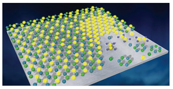
Dosing of ethylene and borazine near a hot iridium surface leads to self-assembly of a two-dimensional structure of graphene in quantum dots. Each dot has a diameter of approx. 2 nm and is surrounded by a two-dimensional alloy of boron, nitrogen, and carbon atoms.
At DTU, Professor Peter Bøggild is equally thrilled and believes that the new discovery has a huge potential.
“We know that patterning of thin films is one of the keys to produce new properties, and—in my opinion—this is a breakthrough. We already know how we can stack materials one layer at a time, and now it appears that we can also pattern them in something approaching atomic resolution. It will be exciting to see how far we can get with this strategy.”
Controlled formation process
The researchers discovered that the distance between the graphene islands can be ‘programmed’ by controlling the gas concentration and temperature during the formation of the thin layers. This opens up entirely new opportunities for the future production of nano-sized lithographic patterns.
Peter Bøggild believes, however, that it is still too early to say anything about the applications.
“We’ve basically discovered a new way of controlling nanomaterials at atomic scale. Graphene islands behave like small artificial atoms and can be used for many different applications within the energy sector, biosensors, and optoelectronics. But where it gets really exciting is if we can learn to do the same with some of the hundreds of other atom-thin films that we know today—to get them to self-assemble as complex structures is a ‘holy grail’ in this research field,” says Peter Bøggild.
Share on:


Suggested Items
LQDX Divests Aluminum Soldering Business - Mina™ - to Taiyo America Inc.
05/02/2024 | PRNewswireLQDX, formerly known as Averatek Corp., developer of high-performance materials for advanced semiconductor manufacturing, today announced that it has divested its aluminum soldering business – known as MinaTM – to Taiyo America Inc., a global market leader in advanced electronic materials.
Indium Corporation Expert to Present on Pb-Free Solder for Die-Attach in Discrete Power Applications
04/30/2024 | Indium CorporationIndium Corporation Product Manager – Semiconductor Dean Payne will present at the Advanced Packaging for Power Electronics conference, hosted by IMAPS, held May 8-9 in Woburn, Massachusetts, USA.
Real Time with... IPC APEX EXPO 2024: Adhesive Materials and Equipment Update with Dymax
05/01/2024 | Real Time with...IPC APEX EXPOVirginia Hogan, global business development manager at Dymax, discusses adhesive materials, dispensing and curing equipment, a new, high-reliability conformal coating, and various materials and dispensing methods.
Real Time with... IPC APEX EXPO 2024: Sustainability in the Industry
04/26/2024 | Real Time with...IPC APEX EXPOGuest Editor Henry Crandall and Chris Nash of Indium Corporation discuss the company's 90th anniversary and its focus on sustainability. They focus on the benefits of sustainable materials, their compatibility, and value propositions. The conversation also highlights how Durafuse LT technology's role in reducing reflow temperatures is leading to significant cost and energy savings. Nash also touches on downstream sustainability efforts such as using recycled materials for packaging.
SMC Korea 2024 to Highlight Semiconductor Materials Trends and Innovations on Industry’s Path to $1 Trillion
04/24/2024 | SEMIWith Korea a major consumer of semiconductor materials and advanced materials a key driver of innovation on the industry’s path to $1 trillion, industry leaders and experts will gather at SMC (Strategic Materials Conference) Korea 2024 on May 29 at the Suwon Convention Center in Gyeonggi-do, South Korea to provide insights into the latest materials developments and trends. Registration is open.