


 The Chemical Connection: Reducing Etch System Water Usage, Part 2
 It’s Only Common Sense: Nice Guys Really Can Finish First
 The Right Approach: I Hear the Train A Comin'
A Simple Soak for a Solar Tune-Up
November 13, 2017 | KAUSTEstimated reading time: 2 minutes
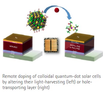
The performance of solar cells that consist of semiconductor nanoparticles surrounded by ligand molecules is now easier to control. Researchers from KAUST have developed a method that enhances the ability of these colloidal quantum dot (CQD) solar cells to convert the sun’s energy into electricity by altering the surface chemistry of their functional layers in a noninvasive way1, 2.
CQDs, such as lead sulfide, are readily processed in solution and benefit from highly tunable and narrow light-emission ranges, depending on their size and composition. “This makes them compelling building blocks for light-harvesting, detection, and emission technologies,” says materials engineer, Aram Amassian, who led the team. Recent breakthroughs in solution-phase exchange and device engineering, such as large-area, lost-cost techniques that use ink-based coating and printing for material deposition, mean that CQD solar cells hold potential for high-performance photovoltaic devices.
The CQD surface chemistry serves multiple, simultaneous and often competing purposes: these include stabilizing the colloidal ink and maintaining nanoparticle cohesion in the solid. However, according to Amassian, existing approaches cannot fully passivate or dope CQDs without inadvertently affecting other properties, especially their photovoltaic response. “Chemical modifications also tend to involve intricate surface chemistry,” he adds.
In response, Amassian’s team, in collaboration with Georgia Institute of Technology, USA, and the University of Toronto, Canada, has devised a mild, single-step approach that incorporates molecular dopants into solar cells. “The dopant molecules do not chemically bind to the CQD surface but remotely transfer charges to it,” explains PhD candidate Ahmad R. Kirmani, who selected the molecules and designed the protocols.
“All nanocrystal films, even the most closely packed ones used in state-of-the-art CQD solar cells, have nanoscale pathways through which molecules of the right size can diffuse,” explains Amassian. The researchers soaked the solar cells in the dopant solution for an optimum time, allowing dopant molecules to travel through these pathways. The dopants effectively tuned electron and hole concentrations in the layers while passivating electronic defects.
“A key difficulty was to have a simple process without compromising doping efficiency,” says Kirmani, noting that choosing a suitable solvent and determining the needed amount of dopant molecules helped him optimize the process.
Amassian’s team demonstrated that their approach can apply to different CQD solar-cell materials, functional layers and device architectures. Specifically, their protocols promoted electron transport in the light-harvesting layer1 or limited electron back-flow into its contiguous hole-transporting counterpart2.
The team is now investigating the scalable, low-cost manufacturing of CQD solar cells in ambient air—a major hurdle to commercialization. Typical fabrication methods demand expensive, controlled humidity conditions to achieve cell stability and efficiency. The researchers are studying the role of the hole-transporting layer under ambient manufacturing conditions and the subsequent device stability.
Share on:


Suggested Items
Real Time with… IPC APEX EXPO 2024: Exploring the Future of Surface Finishes
04/25/2024 | Real Time with...IPC APEX EXPOJoe McGurran, product marketing director for MKS Atotech, looks into the future of surface finishes, discussing less nickel, reduced thickness, technologies influencing HDI and UHDI, and the benefits of nickel-free surface finishes. He also touches on popular finishes like ENIG and palladium immersion gold and discusses the value proposition of making a change.
Designer’s Notebook: What Designers Need to Know About Manufacturing, Part 2
04/24/2024 | Vern Solberg -- Column: Designer's NotebookThe printed circuit board (PCB) is the primary base element for providing the interconnect platform for mounting and electrically joining electronic components. When assessing PCB design complexity, first consider the component area and board area ratio. If the surface area for the component interface is restricted, it may justify adopting multilayer or multilayer sequential buildup (SBU) PCB fabrication to enable a more efficient sub-surface circuit interconnect.
IDTechEx Report Unveils 3D Electronics Status and Opportunities
04/22/2024 | PRNewswire3D electronics is an emerging manufacturing approach that enables electronics to be integrated within or onto the surface of objects. 3D electronic manufacturing techniques empower new features, including mass customizability, greater integration, and improved sustainability in the electronics industry.
NASA, Japan Advance Space Cooperation, Sign Agreement for Lunar Rover
04/11/2024 | NASANASA Administrator Bill Nelson and Japan’s Minister of Education, Culture, Sports, Science and Technology (MEXT) Masahito Moriyama have signed an agreement to advance sustainable human exploration of the Moon.
Lockheed Martin Conducts Historic LRASM Flight Test
04/04/2024 | Lockheed MartinThe U.S. Navy in partnership with Lockheed Martin [NYSE: LMT] successfully conducted a historic Long-Range Anti-Ship Missile (LRASM) flight test with four missiles simultaneously in flight.