


 The Chemical Connection: Reducing Etch System Water Usage, Part 2
 It’s Only Common Sense: Nice Guys Really Can Finish First
 The Right Approach: I Hear the Train A Comin'
A Chip for Environmental and Health Monitoring
December 18, 2017 | FAUEstimated reading time: 3 minutes
Sensors for incorporation in inexpensive measuring devices or virtual personal support systems are increasingly in demand in the environmental, safety, and health-monitoring fields.
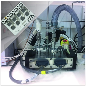
Image caption: In a previous project in which they collaborated with Israeli colleagues, FAU scientists developed intelligent sensor arrays that can analyse complex gas mixtures. The sensors are positioned on the chip-like box (top left) and the analysis of the gas composition is performed by the structure in the large image. In the new project CC-Sens, the researchers are aiming to integrate the sensor elements with all the electronics on a single chip and miniaturise the result. The number of sensor fields (the eight rectangles on the ‘chip’) will then be significantly increased. (Image: Technion/Laboratory for nanomaterial-based devices)
To date, however, progress has been hampered because the cost-effective manufacturing processes necessary for mass production are lacking. Researchers at FAU with international partners from Israel and Germany have set about changing this in a project funded by the German Federal Ministry of Education and Research. If the project is successful, the sensors could in future be used for large-scale close monitoring of NO2 levels in metropolitan areas and to improve the diagnosis and early detection of cancers.
Combining different sensor components is a key factor
The project represents an extension of an earlier successful collaborative undertaking in which the Erlangen-based team developed the technological groundwork together with their Israeli colleagues. These include intelligent sensor arrays, which can analyse complex gas mixtures. To do this, the scientists combined several sensor components which react to large numbers of molecules in non-specific but slightly different ways. ‘Based on the combined reactions of all sensor components, we can deduce the presence of a specific molecule,’ explains Prof. Silke Christiansen, who is working with Prof. Gerd Leuchs, Professor of Experimental Physics (Optics) at FAU and the director of the Max Planck Institute for the Science of Light. The researchers have already successfully tested the concept underlying the sensor in the diagnosis of cancer – but using a design which is not yet suitable for cost-effective mass production.
Two challenges – miniaturisation and compatibility
To produce their miniaturised sensor arrays, the researchers first need to overcome two challenges. Firstly, they have to integrate the three main components in a single chip – the gas-sensitive sensors, the transistors for processing the signals and artificial intelligence in the form of neural networks, which process the complex sensor signal patterns and evaluate them. The second problem is that the researchers are restricted in terms of the materials they can use. ‘In order to achieve industrial-scale mass production, the sensor arrays will have to be made on the large assembly lines that are already being employed for the extensive manufacture of microchips, but these are customised to the types of manufacturing processes needed to produce semiconductor devices. If we are to use them, only certain materials can be used, since atypical components can permanently contaminate these kinds of plants,’ said Christiansen.
FAU – an expert in material analysis and processing
The FAU team is working on the project – which has attracted total funding of €1.8 million – alongside three Israeli participants and a German partner from industry. The project partners are the Israeli semiconductor manufacturer Tower Semiconductor, Technion in Haifa, Tel Aviv University and the German semiconductor manufacturing plant construction company Singulus Technologies AG, based in Kahl am Main. The scientists at the Chair of Experimental Physics (Optics) are contributing their expertise in the field of materials analysis and processing. ‘In our lab we will be investigating whether the materials we use actually work as they are supposed to, and how the production processes will need to be adapted to create sensor structures that function properly,’ explains Prof. Christiansen.
In addition, the researchers will be fine-tuning the functionality of the materials used. This will allow, for example, organic molecules for specific sensor applications to be applied to the substrate of the chip, which will provide characteristic sensor responses in specific areas of application, such as in the respiratory diagnosis of cancer or monitoring levels of harmful gases in the environment or workplaces.
Share on:


Suggested Items
LQDX Divests Aluminum Soldering Business - Mina™ - to Taiyo America Inc.
05/02/2024 | PRNewswireLQDX, formerly known as Averatek Corp., developer of high-performance materials for advanced semiconductor manufacturing, today announced that it has divested its aluminum soldering business – known as MinaTM – to Taiyo America Inc., a global market leader in advanced electronic materials.
Indium Corporation Expert to Present on Pb-Free Solder for Die-Attach in Discrete Power Applications
04/30/2024 | Indium CorporationIndium Corporation Product Manager – Semiconductor Dean Payne will present at the Advanced Packaging for Power Electronics conference, hosted by IMAPS, held May 8-9 in Woburn, Massachusetts, USA.
Real Time with... IPC APEX EXPO 2024: Adhesive Materials and Equipment Update with Dymax
05/01/2024 | Real Time with...IPC APEX EXPOVirginia Hogan, global business development manager at Dymax, discusses adhesive materials, dispensing and curing equipment, a new, high-reliability conformal coating, and various materials and dispensing methods.
Real Time with... IPC APEX EXPO 2024: Sustainability in the Industry
04/26/2024 | Real Time with...IPC APEX EXPOGuest Editor Henry Crandall and Chris Nash of Indium Corporation discuss the company's 90th anniversary and its focus on sustainability. They focus on the benefits of sustainable materials, their compatibility, and value propositions. The conversation also highlights how Durafuse LT technology's role in reducing reflow temperatures is leading to significant cost and energy savings. Nash also touches on downstream sustainability efforts such as using recycled materials for packaging.
SMC Korea 2024 to Highlight Semiconductor Materials Trends and Innovations on Industry’s Path to $1 Trillion
04/24/2024 | SEMIWith Korea a major consumer of semiconductor materials and advanced materials a key driver of innovation on the industry’s path to $1 trillion, industry leaders and experts will gather at SMC (Strategic Materials Conference) Korea 2024 on May 29 at the Suwon Convention Center in Gyeonggi-do, South Korea to provide insights into the latest materials developments and trends. Registration is open.