


 The Marketing Minute: Marketing With Layers
 The Right Approach: Electro-Tek—A Williams Family Legacy, Part 1
 It’s Only Common Sense: If You’re Not Differentiated, You’re Dead


Sensor the Size of a Nitrogen Atom Investigates Hard Drives
January 2, 2018 | Fraunhofer Institute for Applied Solid State PhysicsEstimated reading time: 4 minutes
Integrated circuitry is becoming increasingly complex. These days a Pentium processor contains some 30 million transistors. And the magnetic structures found in hard drives measure just 10 to 20 nanometers across – less than a flu virus at 80 to 120 nanometers in diameter.
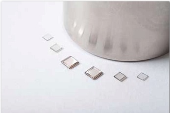
Ultra-pure diamonds produced at Fraunhofer IAF for quantum applications. (Image: Fraunhofer IAF)
Dimensions are rapidly approaching the realm of quantum physics and, already, researchers at the Fraunhofer Institute for Applied Solid State Physics IAF in Freiburg are applying themselves to the quantum technology challenges of tomorrow. Together with colleagues at the Max Planck Institute for Solid State Research, they are developing a quantum sensor that will be able to precisely measure the tiny magnetic fields we can expect to see in the next generation of hard discs. The sensor itself is just slightly larger than a nitrogen atom, with a synthetic diamond to act as a substrate.
Diamond has a variety of advantages quite apart from its considerable mechanical and chemical stability. For instance, one can implant foreign atoms such as boron or phosphorus, thereby turning the crystals into semiconductors. Diamond is also the perfect material for optical circuits. But perhaps its greatest attribute is its impressive thermal conductivity, with the strength of the carbon atom bonds ensuring that heat is rapidly dissipated.
Over the past decades, Fraunhofer IAF has developed optimized systems for producing diamonds. The process for mass production takes places in a plasma reactor, and Freiburg possesses many of these silver-colored devices. Plasma is ignited to generate temperatures of 800 to 900 degrees Celsius so that, when gas is fed into the chamber, diamond layers can form on the square-shaped substrate. The diamond crystals have an edge length of between three and eight millimeters, and are then separated from the substrate and polished using a laser.
The special ellipsoid form of the plasma reactor developed at Fraunhofer IAF allows for large-scale diamond separation. (Image: Fraunhofer IAF)
Preparing the diamond to act as a magnetic detector
Manufacturing the innovative quantum sensor requires a particularly pure crystal, which has inspired further improvements in the process. For instance, in order to grow ultra-pure diamond layers, the methane that provides the carbon for the diamond is pre-filtered using a zirconium filter.
On top of that, the gas must be isotopically pure, since only 12C – a stable isotope of the carbon atom – has zero nuclear spin, which is a prerequisite for the magnetic sensor later on. The hydrogen also undergoes a purification process, after which the ultra-pure single crystal diamond must be prepared for its role as a magnetic detector. Here there are two options: either you insert a single nitrogen atom into the extremely fine tip, or you add nitrogen at the final phase of the diamond production process.
After that, the diamond tip is honed in oxygen plasma using an etching process in the institute’s own cleanroom. The final result is an extremely fine diamond tip that resembles that of an atomic force microscope. The key to the whole design is the added nitrogen atom together with a neighboring vacancy in the crystal structure.
This combined nitrogen-vacancy center acts as the actual sensor, emitting light when it is exposed to a laser and microwaves. If there is a magnet nearby, it will vary in its light emission. Experts call this electron spin resonance spectroscopy. Not only can this technique detect magnetic fields with nanometer accuracy, it can determine their force as well, opening up an extraordinary range of applications.
For instance, the tiny diamond tips can be used to monitor hard drive quality. These data storage devices are tightly packed and there are always tiny errors. The quantum sensor can identify defective data segments so that they are excluded from the disc reading and writing process. This reduces the defect rate, which is soaring as miniaturization continues apace, and cuts down on production costs.
Quantum sensors could measure brain activity
The tiny sensor can potentially be applied in a wide range of scenarios, since there are weak magnetic fields everywhere, even in the brain.
“Whenever electrons move, they generate a magnetic field,” says IAF expert Christoph Nebel. So when we think or feel, our brains are generating magnetic fields.
Researchers are keen to localize this brain activity to determine the areas of the brain that are responsible for a certain function or feeling. This can be done directly by measuring brainwaves using electrodes, but the results are very imprecise. Magnetic field measurements offer far better results.
However, the sensors in use at the moment have one significant disadvantage in that they must be cooled with liquid nitrogen. Drawing on the extreme thermal conductivity of diamond, the new technology can operate at room temperature without the need for any cooling. For this application, instead of using fine tips you would use tiny platelets that incorporate multiple nitrogen-vacancy centers. Each center supplies a point in the image and, together, a detailed picture.
Currently, however, Christoph Nebel and his team are focusing their attention on researching and optimizing diamond as a high-tech material. This application in quantum sensor technology is a promising beginning.
Share on:


Testimonial
"The I-Connect007 team is outstanding—kind, responsive, and a true marketing partner. Their design team created fresh, eye-catching ads, and their editorial support polished our content to let our brand shine. Thank you all! "
Sweeney Ng - CEE PCBSuggested Items
The Marketing Minute: Marketing With Layers
10/15/2025 | Brittany Martin -- Column: The Marketing MinuteMarketing to a technical audience is like crafting a multilayer board: Each layer serves a purpose, from the surface story to the buried detail that keeps everything connected. At I-Connect007, we’ve learned that the best marketing campaigns aren’t built linearly; they’re layered. A campaign might start with a highly technical resource, such as an in-depth article, a white paper, or a podcast featuring an engineer delving into the details of a process. That’s the foundation, the substance that earns credibility.
Taking Control of PCB Verification One Step at a Time
10/09/2025 | Kirk Fabbri, Siemens EDAToday’s designs are as complex as ever, and engineers face tough decisions every day. Simulation and verification teams are confronted with a three-fold challenge: understanding the underlying theory, mastering the tools, and applying best practices.Engineers need to navigate a vast and ever-changing cast of design and simulation tools, often with overlapping functionality.
Happy’s Tech Talk #43: Engineering Statistics Training With Free Software
10/06/2025 | Happy Holden -- Column: Happy’s Tech TalkIn over 50 years as a PCB process engineer, the one skill I acquired in college that has been most beneficial is engineering statistics. Basic statistics was part of my engineering fundamentals classes, but I petitioned the dean to let me take the engineering statistics graduate course because I was creating a senior thesis for my honors focus and needed more training on Design of Experiments (DOE).
Connect the Dots: Evolution of PCB Manufacturing—Lamination
10/02/2025 | Matt Stevenson -- Column: Connect the DotsWhen I wrote The Printed Circuit Designer's Guide to...™ Designing for Reality, it was not a one-and-done effort. Technology is advancing rapidly. Designing for the reality of PCB manufacturing will continue to evolve. That’s why I encourage designers to stay on top of the tools and processes used during production, to ensure their designs capitalize on the capabilities of their manufacturing partner.
Empower Sets New Benchmark with 20x Faster Response and Breakthrough Sustainability Demonstrated at OCP Global Summit 2025
09/25/2025 | Empower SemiconductorEmpower Semiconductor, the world leader in powering AI-class processors, announced that its Crescendo chipset, an artificial intelligence (AI) and high-performance computing (HPC) processor true vertical power delivery platform, is available now for final sampling, with mass production slated for late 2025.