


 It’s Only Common Sense: Nice Guys Really Can Finish First
 The Right Approach: I Hear the Train A Comin'
 Marcy's Musings: The Growing Industry
Diamonds Show Promise for Spintronic Devices
January 30, 2018 | AIP.orgEstimated reading time: 2 minutes
Conventional electronics rely on controlling electric charge. Recently, researchers have been exploring the potential for a new technology, spintronics, that relies on detecting and controlling a particle's spin. This technology could lead to new types of more efficient and powerful devices.
In a paper published in Applied Physics Letters, from AIP Publishing, researchers measured how strongly a charge carrier's spin interacts with a magnetic field in diamond. This crucial property shows diamond as a promising material for spintronic devices.
Diamond is attractive because it would be easier to process and fabricate into spintronic devices than typical semiconductor materials, said Golrokh Akhgar, a physicist at La Trobe University in Australia. Conventional quantum devices are based on multiple thin layers of semiconductors, which require an elaborate fabrication process in an ultrahigh vacuum.
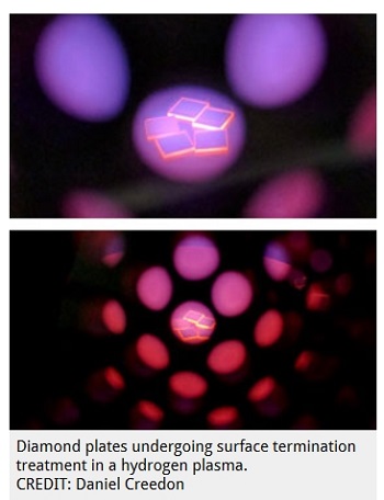
"Diamond is normally an extremely good insulator," Akhgar said. But, when exposed to hydrogen plasma, the diamond incorporates hydrogen atoms into its surface. When a hydrogenated diamond is introduced to moist air, it becomes electrically conductive because a thin layer of water forms on its surface, pulling electrons from the diamond. The missing electrons at the diamond surface behave like positively charged particles, called holes, making the surface conductive.
Researchers found that these holes have many of the right properties for spintronics. The most important property is a relativistic effect called spin-orbit coupling, where the spin of a charge carrier interacts with its orbital motion. A strong coupling enables researchers to control the particle's spin with an electric field.
In previous work, the researchers measured how strongly a hole's spin-orbit coupling could be engineered with an electric field. They also showed that an external electric field could tune the strength of the coupling.
In recent experiments, the researchers measured how strongly a hole's spin interacts with a magnetic field. For this measurement, the researchers applied constant magnetic fields of different strengths parallel to the diamond surface at temperatures below 4 Kelvin. They also simultaneously applied a steadily varying perpendicular field. By monitoring how the electrical resistance of the diamond changed, they determined the g-factor. This quantity could help researchers control spin in future devices using a magnetic field.
"The coupling strength of carrier spins to electric and magnetic fields lies at the heart of spintronics," Akhgar said. "We now have the two crucial parameters for the manipulation of spins in the conductive surface layer of diamond by either electric or magnetic fields."
Additionally, diamond is transparent, so it can be incorporated into optical devices that operate with visible or ultraviolet light. Nitrogen-vacancy diamonds -- which contain nitrogen atoms paired with missing carbon atoms in its crystal structure -- show promise as a quantum bit, or qubit, the basis for quantum information technology. Being able to manipulate spin and use it as a qubit could lead to yet more devices with untapped potential, Akhgar said.
Share on:


Suggested Items
Real Time with… IPC APEX EXPO 2024: Exploring the Future of Surface Finishes
04/25/2024 | Real Time with...IPC APEX EXPOJoe McGurran, product marketing director for MKS Atotech, looks into the future of surface finishes, discussing less nickel, reduced thickness, technologies influencing HDI and UHDI, and the benefits of nickel-free surface finishes. He also touches on popular finishes like ENIG and palladium immersion gold and discusses the value proposition of making a change.
Designer’s Notebook: What Designers Need to Know About Manufacturing, Part 2
04/24/2024 | Vern Solberg -- Column: Designer's NotebookThe printed circuit board (PCB) is the primary base element for providing the interconnect platform for mounting and electrically joining electronic components. When assessing PCB design complexity, first consider the component area and board area ratio. If the surface area for the component interface is restricted, it may justify adopting multilayer or multilayer sequential buildup (SBU) PCB fabrication to enable a more efficient sub-surface circuit interconnect.
IDTechEx Report Unveils 3D Electronics Status and Opportunities
04/22/2024 | PRNewswire3D electronics is an emerging manufacturing approach that enables electronics to be integrated within or onto the surface of objects. 3D electronic manufacturing techniques empower new features, including mass customizability, greater integration, and improved sustainability in the electronics industry.
NASA, Japan Advance Space Cooperation, Sign Agreement for Lunar Rover
04/11/2024 | NASANASA Administrator Bill Nelson and Japan’s Minister of Education, Culture, Sports, Science and Technology (MEXT) Masahito Moriyama have signed an agreement to advance sustainable human exploration of the Moon.
Lockheed Martin Conducts Historic LRASM Flight Test
04/04/2024 | Lockheed MartinThe U.S. Navy in partnership with Lockheed Martin [NYSE: LMT] successfully conducted a historic Long-Range Anti-Ship Missile (LRASM) flight test with four missiles simultaneously in flight.