


 Dan’s Biz Bookshelf: ‘Abundance: How We Build a Better Future’
 Trouble in Your Tank: In Complex Systems, Design Rules Aren’t Optional
 It’s Only Common Sense: The Phone Is Still Your Competitive Advantage


Nordson MARCH's New Plasma Systems Enable Very High Throughput Processing for 3D and Wafer-level Package Assembly
February 1, 2018 | Nordson MARCHEstimated reading time: 2 minutes
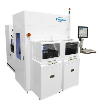
Nordson MARCH, a Nordson company (NASDAQ: NDSN), a global leader in plasma processing technology, introduces the MesoSPHERE™ Plasma System for very-high throughput processing of 3D and wafer-level packaging processes such as fan-in, fan-out, wafer-level, and panel-level -handling wafers up to 450mm and panels up to 480mm. The MesoSPHERE's new, patented W3 three-axis symmetrical plasma chamber ensures that all areas of the wafer are treated equally and uniformly. Tight control over all process parameters gives highly repeatable results.
For wafer cleaning, the MesoSPHERE plasma system removes contamination prior to wafer bumping, organic contamination, fluorine and other halogen contamination, and metal and metal oxides. Plasma improves spun-on film adhesion and cleans metallic bond pads.
For wafer etching, the MesoSPHERE plasma system descums wafers of residual photoresist and BCB, pattern dielectric layers for redistribution, strip/etch photoresist, enhances adhesion of wafer applied materials, removes excess wafer applied mold /epoxy, enhances adhesion of gold solder bumps, destresses wafer to reduce breakage, improves spun-on film adhesion, and cleans aluminum bond pads.
The MesoSPHERE's chamber design and control architecture enable short plasma cycle times with very low overhead, maximizing throughput and minimizing cost of ownership. Plasma confinement technology uses a ring to isolate and focus plasma so it's distributed directly above the wafer, minimizing undesired secondary reactions. Process temperatures can be kept low because the ring increases etch rate capability without increasing the electrode temperature or adding bias to the chuck.
An innovative handling system transfers round or square substrates and frame or bonded carriers. The modular design allows capacity increase on a per plasma chamber basis. Equipment front end module (EFEM) integration supports from 1 to 4 plasma chambers. A pocket chuck design provides accurate substrate placement and centering, for additional process repeatability.
"A unique feature of the MesoSPHERE is the way we developed the isolation," explained Jonathan Doan, director of marketing for Nordson MARCH. "It allows our customers a method to perform advanced packaging without having to use an expensive carrier and it can be used with 300mm wafers on frames."
About Nordson MARCH
Nordson MARCH designs and manufactures a complete line of award-winning and patented plasma treatment systems that improve product reliability and increase production yields. Delivering over 30 years of continuous innovation Nordson MARCH is a global leader in plasma processing technology for manufacturing semiconductors, printed circuit boards, microelectronics, and medical devices with offices and labs worldwide, including the USA, Europe, Singapore, China, Japan, and Korea. An expert staff of scientists and engineers is available to assist development of plasma processes. For more information, click here.
About Nordson Corporation
Nordson Corporation engineers, manufactures and markets differentiated products and systems that dispense, apply and control adhesives, coatings, polymers, sealants, biomaterials, and other fluids, test and inspect for quality, and treat and cure surfaces, and are supported by application expertise and direct global sales and service. Nordson serves many consumer non-durable, durable and technology end-markets including packaging, nonwovens, electronics, medical, appliances, energy, transportation, construction, and general product assembly and finishing. Founded in 1954, headquartered in Westlake, Ohio, Nordson has operations and support offices in nearly 40 countries.
Share on:


Subscribe
Stay ahead of the technologies shaping the future of electronics with our latest newsletter, Advanced Electronics Packaging Digest. Get expert insights on advanced packaging, materials, and system-level innovation, delivered straight to your inbox.
Subscribe now to stay informed, competitive, and connected.
Suggested Items
BGA Technology Expands Inspection Capabilities with Creative Electron TruView X-ray System
05/08/2026 | BGA TechnologyBGA Technology, a leading provider of advanced electronics testing and inspection services, has enhanced its inspection capabilities with the addition of a Creative Electron TruView™ Simplex X-ray system at its Holbrook, New York facility.
AQUANOX A4727 and A4625 Lead KYZEN Offerings at SMTA Oregon Expo and Tech Forum
05/06/2026 | KYZENKYZEN, the global leader in innovative environmentally responsible cleaning chemistries, will exhibit at the SMTA Oregon Expo and Tech Forum scheduled to take place Thursday, May 19 at the Wingspan Event and Conference Center in Hillsboro, Oregon.
Connect the Dots: Designing for the Future of Manufacturing Reality—Surface Finish
05/07/2026 | Matt Stevenson -- Column: Connect the DotsWhen designing the complex boards that many electronic devices require to operate, designers should consider manufacturability at every step. This is my last article focused on designing for the always-evolving manufacturing reality. Choosing the right surface finish has always been important. If you are creating intricate designs with a wide variety of components, like for an ultra-high density interconnect (UHDI) board, surface finish is a critical last step.
Indium to Showcase High-Performance AI Application Solutions at SEMICON SEA 2026
05/01/2026 | Indium CorporationAs a leading provider of advanced materials solutions for today’s demanding AI applications, Indium Corporation® will feature its high-reliability product portfolio at SEMICON SEA 2026, May 5-7, in Kuala Lumpur, Malaysia.
ACCM Unveils Negative and Near-zero CTE Materials for Large-Format AI Chips
04/21/2026 | Advanced Chip and Circuit MaterialsAdvanced Chip and Circuit Materials, Inc. (ACCM) has launched two new materials: Celeritas HM50, with a negative coefficient of thermal expansion (CTE) of -8 ppm/°C to offset the positive CTE and expansion of copper with temperature on circuit boards, and Celeritas HM001, with near-zero CTE and the low-loss performance needed for high-speed signal layers to 224 Gb/s and faster in artificial intelligence (AI) circuits.