


 The Chemical Connection: Reducing Etch System Water Usage, Part 2
 It’s Only Common Sense: Nice Guys Really Can Finish First
 The Right Approach: I Hear the Train A Comin'
Scalable Two-Dimensional Materials Advance Future-Gen Electronics
February 15, 2018 | Pennsylvania State UniversityEstimated reading time: 3 minutes
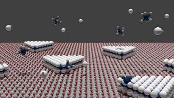
Since the discovery of the remarkable properties of graphene, scientists have increasingly focused research on the many other two-dimensional materials possible, both those found in nature and those concocted in the lab. However, growing high-quality, crystalline 2-D materials at scale has proven a significant challenge.
A pair of papers published online in two nanotechnology journals recently provide the basis for growing wafer-scale two-dimensional crystals for future electronic devices. In work led by Joan Redwing, director of the National Science Foundation-sponsored Two-Dimensional Crystal Consortium — Materials Innovation Platform, and professor of materials science and engineering and electrical engineering, Penn State, researchers developed a multistep process to make single crystal, atomically thin films of tungsten diselenide across large-area sapphire substrates.
"Up until now, the majority of 2-D devices have been fabricated using small flakes that are exfoliated off of bulk crystals," Redwing said. "To develop a device-ready technology, you have to be able to make devices on large-area substrates and they have to have good crystal quality."
The process uses sapphire as the substrate because of its crystalline structure. This structure orients the film growth in a crystal pattern in a process called epitaxy. As small islands of the material form on the substrate and the substrate is heated, the islands spread out across the substrate in a uniform pattern, forming a large-area film without gaps and with very few defects. The key advance was the use of gas-source chemical vapor deposition to precisely control the island density and rate of spreading to achieve a single layer of the 2-D material.
The researchers published their work, "Diffusion-Controlled Epitaxy of Large Area Coalesced WSe2 Monolayers on Sapphire," in Nano Letters.
In a related paper, "Realizing Large-Scale, Electronic-Grade Two-Dimensional Semiconductors," published online in ACS Nano, a team led by Joshua Robinson, associate professor of materials science and engineering, Penn State, provides the foundational understanding to enable device-ready synthetic 2-D semiconductors based on these epitaxial large-area films in future industrial-scale electronics.
"The primary significance of this work is we were able to achieve an understanding of the extrinsic factors that go into having a high-quality 2-D material," Robinson said. "What we found was that even when you grow oriented crystals on a surface, there are other factors that impact the ability to get high electron mobility or fast transistors."
In particular, they found that there is a strong interaction between the sapphire substrate and the monolayer film, with the substrate dominating the properties. To overcome these challenges, the researchers grew two or three layers, which improved the performance by factors of 20-100 times.
"This is the first real evidence of the effect of the substrate on the transport properties of 2-D layers," Robinson said.
Xiaotian Zhang, a doctoral student in Redwing's group, is first author on the Nano Letters paper. Yu-Chuan Lin, a former doctoral student in Robinson's group, is first author on the paper in ACS Nano. Both Redwing and Robinson are coauthors on both papers and are both members of the Materials Research Institute and the Penn State Two-Dimensional Crystal Consortium — Materials Innovation Platform, a National Science Foundation national user laboratory advancing the state-of-the art in the crystal growth of atomically thin 2-D materials for next-generation electronics (NSF cooperative agreement DMR-1539916).
The Dow Chemical Company, the Semiconductor Research Corporation through the Center for Low Energy Systems Technology (LEAST), and DARPA, the Defense Advanced Research Projects Administration, supported this work, in addition to NSF.
Twenty-two authors from four universities contributed to the ACS Nano paper, which reported on four years of research. Ten authors contributed to the Nano Letters paper, from both Penn State and Rensselaer Polytechnic Institute. Robinson would like to acknowledge Susan K. Fullerton's group from University of Pittsburgh for valuable contributions to the electrical section of the ACS Nano paper.
Share on:


Suggested Items
LQDX Divests Aluminum Soldering Business - Mina™ - to Taiyo America Inc.
05/02/2024 | PRNewswireLQDX, formerly known as Averatek Corp., developer of high-performance materials for advanced semiconductor manufacturing, today announced that it has divested its aluminum soldering business – known as MinaTM – to Taiyo America Inc., a global market leader in advanced electronic materials.
Indium Corporation Expert to Present on Pb-Free Solder for Die-Attach in Discrete Power Applications
04/30/2024 | Indium CorporationIndium Corporation Product Manager – Semiconductor Dean Payne will present at the Advanced Packaging for Power Electronics conference, hosted by IMAPS, held May 8-9 in Woburn, Massachusetts, USA.
Real Time with... IPC APEX EXPO 2024: Adhesive Materials and Equipment Update with Dymax
05/01/2024 | Real Time with...IPC APEX EXPOVirginia Hogan, global business development manager at Dymax, discusses adhesive materials, dispensing and curing equipment, a new, high-reliability conformal coating, and various materials and dispensing methods.
Real Time with... IPC APEX EXPO 2024: Sustainability in the Industry
04/26/2024 | Real Time with...IPC APEX EXPOGuest Editor Henry Crandall and Chris Nash of Indium Corporation discuss the company's 90th anniversary and its focus on sustainability. They focus on the benefits of sustainable materials, their compatibility, and value propositions. The conversation also highlights how Durafuse LT technology's role in reducing reflow temperatures is leading to significant cost and energy savings. Nash also touches on downstream sustainability efforts such as using recycled materials for packaging.
SMC Korea 2024 to Highlight Semiconductor Materials Trends and Innovations on Industry’s Path to $1 Trillion
04/24/2024 | SEMIWith Korea a major consumer of semiconductor materials and advanced materials a key driver of innovation on the industry’s path to $1 trillion, industry leaders and experts will gather at SMC (Strategic Materials Conference) Korea 2024 on May 29 at the Suwon Convention Center in Gyeonggi-do, South Korea to provide insights into the latest materials developments and trends. Registration is open.