


 The Chemical Connection: Reducing Etch System Water Usage, Part 2
 It’s Only Common Sense: Nice Guys Really Can Finish First
 The Right Approach: I Hear the Train A Comin'
Splitting Crystals for 2D Metallic Conductivity
February 22, 2018 | Tohoku UniversityEstimated reading time: 2 minutes
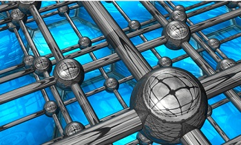
Adding oxygen atoms to a perovskite-like crystal material splits it into layers, giving it unique electrical properties.
Sheets of electrons that are highly mobile in only two dimensions, known as 2D electron gas, have unique properties that can be leveraged for faster and novel electronic devices. Researchers have been exploring 2D electron gas, which was only discovered in 2004, to see how it can be used in superconductors, actuators, and electronic memory devices, among others.
Researchers at Japan's Tohoku University, with an international team of colleagues, recently identified the atomic structure of a group of perovskite-related materials showing interesting 2D conductive properties.
The materials are made of strontium, niobium and oxygen atoms, with a layered structure derived from perovskite. These strontium niobate compounds show promise for developing advanced electronics because of their 'quasi-one-dimensional' metallic conductivity.
Yuichi Ikuhara of Tohoku University's Advanced Institute for Materials Research with Johannes Georg Bednorz of Zürich Research Laboratory and colleagues used atom-resolved scanning transmission electron microscopy combined with theoretical calculations to learn how adding oxygen atoms to strontium niobates affects their conductivity. Four different materials formed depending on the concentration of oxygen atoms.
The scanning transmission electron micrograph shows that the atomic structure was alternately arranged in the three-layer and the zig-zag two-layer thick chain-like slabs, showing quasi-1D metallic conductivity in the former.
The researchers found that three of the materials were conductors of electricity while the fourth was an insulator. At the atomic scale, they discovered the materials were formed of alternating chain-like and zigzag slabs. Depending on the concentration of oxygen atoms, the chain-like slabs were two, three, or four layers thick, sometimes varying within the same material. The zigzag slabs were insulating layers in all the materials, while the chain-like slabs were conducting layers in three of the four materials.
The team determined that local electrical conductivity within the material directly depended on the shapes of the niobate octahedra in the layers. When positive ions of niobium were displaced toward the centers of the niobate octahedra, a local conducting nature was induced.
2D conducting layers are commonly formed by creating an interface between two insulators. It should now be possible to achieve the same goal by segmenting 3D conducting materials into stacks of 2D conducting layers separated by insulating layers, the researchers say in their study published in the journal ACS Nano. This could lead to applications in the development of 2D electrical conducting materials and devices.
Share on:


Suggested Items
LQDX Divests Aluminum Soldering Business - Mina™ - to Taiyo America Inc.
05/02/2024 | PRNewswireLQDX, formerly known as Averatek Corp., developer of high-performance materials for advanced semiconductor manufacturing, today announced that it has divested its aluminum soldering business – known as MinaTM – to Taiyo America Inc., a global market leader in advanced electronic materials.
Indium Corporation Expert to Present on Pb-Free Solder for Die-Attach in Discrete Power Applications
04/30/2024 | Indium CorporationIndium Corporation Product Manager – Semiconductor Dean Payne will present at the Advanced Packaging for Power Electronics conference, hosted by IMAPS, held May 8-9 in Woburn, Massachusetts, USA.
Real Time with... IPC APEX EXPO 2024: Adhesive Materials and Equipment Update with Dymax
05/01/2024 | Real Time with...IPC APEX EXPOVirginia Hogan, global business development manager at Dymax, discusses adhesive materials, dispensing and curing equipment, a new, high-reliability conformal coating, and various materials and dispensing methods.
Real Time with... IPC APEX EXPO 2024: Sustainability in the Industry
04/26/2024 | Real Time with...IPC APEX EXPOGuest Editor Henry Crandall and Chris Nash of Indium Corporation discuss the company's 90th anniversary and its focus on sustainability. They focus on the benefits of sustainable materials, their compatibility, and value propositions. The conversation also highlights how Durafuse LT technology's role in reducing reflow temperatures is leading to significant cost and energy savings. Nash also touches on downstream sustainability efforts such as using recycled materials for packaging.
SMC Korea 2024 to Highlight Semiconductor Materials Trends and Innovations on Industry’s Path to $1 Trillion
04/24/2024 | SEMIWith Korea a major consumer of semiconductor materials and advanced materials a key driver of innovation on the industry’s path to $1 trillion, industry leaders and experts will gather at SMC (Strategic Materials Conference) Korea 2024 on May 29 at the Suwon Convention Center in Gyeonggi-do, South Korea to provide insights into the latest materials developments and trends. Registration is open.