


 Happy’s Tech Talk #28: The Power Mesh Architecture for PCBs
 It’s Only Common Sense: Would You Join Your Own Company?
 The Chemical Connection: Reducing Etch System Water Usage, Part 2
Research Achievement Paves the Way to GaN Power Technology at High Voltages above 650V
April 11, 2018 | ImecEstimated reading time: 3 minutes
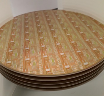
World-leading research and innovation hub in nanoelectronics and digital technologies imec, and fabless technology innovator Qromis, have announced the development of high performance enhancement mode p-GaN power devices on 200mm engineered Coefficient of Thermal Expansion (CTE)-matched substrates, processed in imec’s silicon pilot line. The substrates are offered by Qromis as commercial 200mm QST substrates as part of their patented product portfolio. The results will be presented at next week’s CS international Conference (April 10-11, Brussels, Belgium).
Today, GaN-on-Si technology is the industry standard platform for commercial GaN power switching devices for wafer diameters up to 150mm/6 inch. Imec has pioneered the development of GaN-on-Si power technology for 200mm/8 inch wafers and qualified enhancement mode HEMT and Schottky diode power devices for 100V, 200V and 650V operating voltage ranges, paving the way to high volume manufacturing applications. However, for applications beyond 650V such as electric cars and renewable energy, it has become difficult to further increase the buffer thickness on 200mm wafers to the levels required for higher breakdown and low leakage levels, because of the mismatch in coefficient of thermal expansion (CTE) between the GaN/AlGaN epitaxial layers and the silicon substrate. One can envisage to use thicker Si substrates to keep wafer warp and bow under control for 900V and 1200V applications, but practice has learned that for these higher voltage ranges, the mechanical strength is a concern in high volume manufacturing, and the ever thicker wafers can cause compatibility issues in wafer handling in some processing tools.
Carefully engineered and CMOS fab-friendly QST® substrates with a CTE-matched core having a thermal expansion that very closely matches the thermal expansion of the GaN/AlGaN epitaxial layers, are paving the way to 900V-1200V buffers and beyond, on a standard semi-spec thickness 200mm substrate. Moreover, QST® substrates open perspectives for very thick GaN buffers, including realization of free-standing and very low dislocation density GaN substrates by >100 micron thick fast-growth epitaxial layers. These unique features will enable long awaited commercial vertical GaN power switches and rectifiers suitable for high voltage and high current applications presently dominated by Si IGBTs and SiC power FETs and diodes.
“QST® is revolutionizing GaN technologies and businesses for 200mm and 300mm platforms”, stated Cem Basceri, President and CEO of Qromis. “I am very pleased to see the successful demonstration of high performance GaN power devices by stacking leading edge technologies from Qromis, imec and AIXTRON,” Basceri said.
In this specific collaboration, imec and Qromis developed enhancement mode p-GaN power device specific GaN epitaxial layers on 200mm QST® substrates, with buffers grown in AIXTRON’s G5+ C 200mm high volume manufacturing MOCVD system.
Imec then ported its p-GaN enhancement mode power device technology to the 200mm GaN-on- QST substrates in their silicon pilotline and demonstrated high performance power devices with threshold voltage of 2.8 Volt.
“The engineered QST® substrates from Qromis facilitated a seamless porting of our process of reference from thick GaN-on-Si substrates to standard thickness GaN-on- QST® substrates using the AIX G5+ C system, in a joint effort of imec, Qromis and AIXTRON,” stated Stefaan Decoutere, program director for GaN power technology at imec. The careful selection of the material for the core of the substrates, and the development of the light-blocking wrapping layers resulted in fab-compatible standard thickness substrates and first-time-right processing of the power devices.
Imec acknowledges funding from the Electronic Component Systems for European Leadership Joint Undertaking under grant agreement No 662133, designated as PowerBase.
About imec
Imec is the world-leading research and innovation hub in nanoelectronics and digital technologies. The combination of our widely acclaimed leadership in microchip technology, profound software and ICT expertise is what makes us unique. By leveraging our world-class infrastructure and local and global ecosystem of partners across a multitude of industries, we create groundbreaking innovation in application domains such as healthcare, smart cities and mobility, logistics and manufacturing, energy, and education.
As a trusted partner for companies, start-ups and universities, we bring together close to 3,500 brilliant minds from over 70 nationalities. Imec is headquartered in Leuven, Belgium, and has distributed R&D groups at a number of Flemish universities, in the Netherlands, Taiwan, USA, China, and offices in India and Japan. In 2016, imec’s revenue (P&L) totaled 496 million euro.
Further information about imec can be found here.
Share on:


Suggested Items
Real Time with… IPC APEX EXPO 2024: Innovative Lamination Technology
05/07/2024 | Real Time with...IPC APEX EXPOKevin Barrett of Insulectro and Victor Lazaro of Indubond discuss their companies' partnership, focusing on Indubond's innovative lamination technology that uses induction heating. They discuss the advantages of this technology over traditional methods, its benefits to customers, and the crucial role of automation in manufacturing.
Nolan’s Notes: Coming to Terms With AI
05/07/2024 | Nolan Johnson -- Column: Nolan's NotesHow fast do things move in the world of data analytics? Here’s an example. We’ve been planning this issue on artificial intelligence for the past few months, and, in fact, I had already written this column about a month ago. Then I went to IPC APEX EXPO and upended it all. I originally had compared AI to drag racing in that (CPU) horsepower and new (data) vehicles have steadily delivered higher performance competition. That seemed pretty accurate given how generative AI models dominated the popular media with amazing results—and sometimes spectacular crashes.
DDM Novastar Unveils Affordable NovaPlace Automatic Pick and Place Systems
05/06/2024 | DDM Novastar Inc.DDM Novastar, a prominent U.S. manufacturer specializing in SMT and PCB assembly equipment, proudly announces the recent launch of their NovaPlace Pick & Place systems. This new line introduces entry-level yet high-performance pick and place machines.
May Issue of SMT007 Magazine: Coming to Terms With AI
05/06/2024 | I-Connect007 Editorial TeamIn the May 2024 issue of SMT007 Magazine, we examine the profound effect artificial intelligence and machine learning are having on manufacturing and business processes. We follow technology, innovation, and money as automation becomes the new key indicator of growth in our industry.
iNEMI Names Grace O'Malley CTO
05/02/2024 | iNEMIThe Board of Directors of the International Electronics Manufacturing Initiative (iNEMI) has named Grace O'Malley Chief Technical Officer (CTO).