


 The Chemical Connection: Reducing Etch System Water Usage, Part 2
 It’s Only Common Sense: Nice Guys Really Can Finish First
 The Right Approach: I Hear the Train A Comin'
Surface Engineering Gets the Red Light
April 23, 2018 | KAUSTEstimated reading time: 2 minutes
A method for chemically stabilizing optical nanocrystals, without degrading their electrical properties, has been developed by scientists at KAUST.
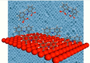
Image caption: Passivating the surface of perovskite nanocrystals with IDA molecules improves their stability and their optical and electrical properties, making them useful for optoelectronic devices.
Halide perovskites are in an exciting class of materials for optoelectronics and photovoltaics. These materials efficiently absorb visible light, possess long charge-carrier diffusion lengths and are easy and cheap to produce. The performance of optical devices can also be improved by incorporating nanometer-scale particles, which have far superior light-emitting and -absorbing properties than the bulk material from which they are derived. So it is unsurprising that scientists are keen to combine these two approaches. The challenge is that tiny perovskite particles aren’t always chemically stable, and their atomic crystal structure is difficult to control.
Attaching molecules, referred to as ligands, can stabilize a nanocrystal. But this so-called passivation can form an electrically insulating shell around the particle that inhibits their effectiveness in electronic devices.
Now, Osman Bakr’s group, and co-workers from KAUST and ShanghaiTech University, has created halide perovskite nanocrystals made from cesium-lead-iodide passivated by 2,2′-iminodibenzoic acid (IDA) ligands. They show that this provides the necessary chemical stability while remaining useful for optoelectronics. And the passivation was simple: just adding IDA powder into the nanocrystal solution and using a centrifuge to remove any excess.
The team chose IDA because it is a bidentate ligand, meaning that it bonds to the nanocrystal at two sites. “The conventional ligands used in these applications, such as oleic acid, are dynamic on the surface of the perovskite nanocrystals and easily come loose,” says Jun Pan, the first author on the paper. “That’s why we apply a double carboxylic group to strongly bind on the surface, which also stabilizes the perovskite crystal phase at room temperature.”
Pan and his team compared the optical properties of both the passivated and unpassivated samples and observed that the treatment improved the photoluminescent quantum yield—a measure of how many photons are emitted for every photon absorbed—from 80 percent to over 95 percent. And while the intensity of light emitted from the unpassivated nanocrystals had dropped significantly five days later, the IDA-treated samples were still emitting light at 90 percent of their initial level 15 days later.
Passivating the surface of perovskite nanocrystals with IDA molecules improves their stability and their optical and electrical properties, making them useful for optoelectronic devices.
The team demonstrated that their stabilized halide perovskite nanocrystals were suitable for optoelectronic applications by using them to build light-emitting diodes. The red-light generating devices again outperformed the unpassivated control device in terms of maximum luminance and luminous power efficiency.
“The next step is to realize more stable perovskite structures and to create an LED with performance above 10 percent based on perovskite nanocrystals,” says Pan.
Share on:


Suggested Items
Real Time with… IPC APEX EXPO 2024: Exploring the Future of Surface Finishes
04/25/2024 | Real Time with...IPC APEX EXPOJoe McGurran, product marketing director for MKS Atotech, looks into the future of surface finishes, discussing less nickel, reduced thickness, technologies influencing HDI and UHDI, and the benefits of nickel-free surface finishes. He also touches on popular finishes like ENIG and palladium immersion gold and discusses the value proposition of making a change.
Designer’s Notebook: What Designers Need to Know About Manufacturing, Part 2
04/24/2024 | Vern Solberg -- Column: Designer's NotebookThe printed circuit board (PCB) is the primary base element for providing the interconnect platform for mounting and electrically joining electronic components. When assessing PCB design complexity, first consider the component area and board area ratio. If the surface area for the component interface is restricted, it may justify adopting multilayer or multilayer sequential buildup (SBU) PCB fabrication to enable a more efficient sub-surface circuit interconnect.
IDTechEx Report Unveils 3D Electronics Status and Opportunities
04/22/2024 | PRNewswire3D electronics is an emerging manufacturing approach that enables electronics to be integrated within or onto the surface of objects. 3D electronic manufacturing techniques empower new features, including mass customizability, greater integration, and improved sustainability in the electronics industry.
NASA, Japan Advance Space Cooperation, Sign Agreement for Lunar Rover
04/11/2024 | NASANASA Administrator Bill Nelson and Japan’s Minister of Education, Culture, Sports, Science and Technology (MEXT) Masahito Moriyama have signed an agreement to advance sustainable human exploration of the Moon.
Lockheed Martin Conducts Historic LRASM Flight Test
04/04/2024 | Lockheed MartinThe U.S. Navy in partnership with Lockheed Martin [NYSE: LMT] successfully conducted a historic Long-Range Anti-Ship Missile (LRASM) flight test with four missiles simultaneously in flight.