


 Happy’s Tech Talk #28: The Power Mesh Architecture for PCBs
 It’s Only Common Sense: Would You Join Your Own Company?
 The Chemical Connection: Reducing Etch System Water Usage, Part 2
Why Perovskite Solar Cells Are So Efficient
April 25, 2018 | KITEstimated reading time: 2 minutes
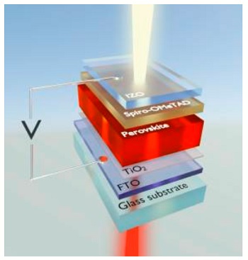
Solar cells with efficiencies above 20% and produced at low costs—perovskites make this possible. Now, researchers of Karlsruhe Institute of Technology (KIT) have gained fundamental insight into the function of perovskite solar cells. They found that bound states of electron-hole pairs can form during the absorption of light. Still, these pairs can be separated easily for current to flow. In addition, they enhance absorption. Perovskites are among the most promising materials for solar cells: When using them, the high efficiency can be combined with low-cost production. Photovoltaics research focuses on halide perovskites that contain both organic and inorganic compounds and, hence, are considered hybrid semiconductors. “In less than one decade, these perovskites underwent an outstanding development. Meanwhile, perovskite solar cells convert more than 20% of the incident light directly into usable current,” says photovoltaics expert Dr. Michael Hetterich of KIT, who coordinates collaboration between KIT and the Center for Solar Energy and Hydrogen Research Baden-Württemberg (ZSW). The vast potential of perovskites is also obvious from tandem solar cells that combine a semitransparent perovskite top cell with a silicon or copper-indium-gallium-diselenide (CIGS) bottom cell. This allows for an optimal use of the solar spectrum.
Current research challenges consist in enhancing the long-term stability of perovskite solar cells and replacing the lead they contain by environmentally more compatible elements. This requires deep insight into the structure and function of the perovskite layers. Researchers of the Institute of Applied Physics and the Light Technology Institute of KIT as well as of ZSW and Ludwig-Maximilians-Universität München study the function of thin-layer tandem solar cells based on perovskites under the CISOVSKIT (development of highly efficient hybrid solar cells from CIGS and perovskite materials) project funded by the Federal Ministry of Education and Research (BMBF). And they obtained new findings relating to the physical nature of the optical transitions.
Optical transitions are changes of the energy state of electrons in a material by emission (release) or absorption (uptake) of photons, i.e. light particles. In his doctoral thesis, Fabian Ruf, who works in the group of Professor Heinz Kalt, KIT, points out that the fundamental optical transition in solar cells with a methyl ammonium lead iodide absorber, the classical halide perovskite, is of excitonic nature. This means that excitons may form in the solar cells after the absorption of light particles. Excitons are bound electron-hole pairs that largely determine the optoelectronic properties. Binding energy of the excitons has to be overcome in order to obtain free charge carriers and to make the current flow.
By means of temperature-dependent electroabsorption spectroscopy, Fabian Ruf studied semitransparent solar cells with methyl ammonium lead iodide absorbers produced by Moritz Schultes of ZSW by a wet chemistry method. The results allow conclusions to be drawn with respect to excitonic transitions over the complete temperature range studied, from 10 Kelvin (-263°C) to room temperature. Depending on the perovskite crystal structure that changes with changing temperature, the exciton binding energy amounts to about 26 and 19 millielectronvolts, respectively. “Hence, the binding energy is small enough to ensure sufficient thermal separation of charge carriers at room temperature,” Michael Hetterich explains. “In addition, the excitonic effects enhance absorption. Both effects together enable efficient operation of the perovskite solar cell.”
Share on:


Suggested Items
The Chemical Connection: Reducing Etch System Water Usage, Part 2
05/02/2024 | Don Ball -- Column: The Chemical ConnectionIn my last column, I reviewed some relatively simple ways to reduce water usage in existing etch systems: cutting down cooling coil water flow, adding chillers to replace plant water for cooling, lowering flow rate nozzles for rinses, etc. This month, I’ll continue with more ways to control water usage in your etcher. Most of these are not easily retrofittable to existing equipment but should be given serious consideration when new equipment is contemplated. With the right combination of add-ons, it is possible to bring the amount of water used in an etch system to almost zero.
Designer’s Notebook: What Designers Need to Know About Manufacturing, Part 2
04/24/2024 | Vern Solberg -- Column: Designer's NotebookThe printed circuit board (PCB) is the primary base element for providing the interconnect platform for mounting and electrically joining electronic components. When assessing PCB design complexity, first consider the component area and board area ratio. If the surface area for the component interface is restricted, it may justify adopting multilayer or multilayer sequential buildup (SBU) PCB fabrication to enable a more efficient sub-surface circuit interconnect.
Insulectro’s 'Storekeepers' Extend Their Welcome to Technology Village at IPC APEX EXPO
04/03/2024 | InsulectroInsulectro, the largest distributor of materials for use in the manufacture of PCBs and printed electronics, welcomes attendees to its TECHNOLOGY VILLAGE during this year’s IPC APEX EXPO at the Anaheim Convention Center, April 9-11, 2024.
ENNOVI Introduces a New Flexible Circuit Production Process for Low Voltage Connectivity in EV Battery Cell Contacting Systems
04/03/2024 | PRNewswireENNOVI, a mobility electrification solutions partner, introduces a more advanced and sustainable way of producing flexible circuits for low voltage signals in electric vehicle (EV) battery cell contacting systems.
Heavy Copper PCBs: Bridging the Gap Between Design and Fabrication, Part 1
04/01/2024 | Yash Sutariya, Saturn Electronics ServicesThey call me Sparky. This is due to my talent for getting shocked by a variety of voltages and because I cannot seem to keep my hands out of power control cabinets. While I do not have the time to throw the knife switch to the off position, that doesn’t stop me from sticking screwdrivers into the fuse boxes. In all honesty, I’m lucky to be alive. Fortunately, I also have a talent for building high-voltage heavy copper circuit boards. Since this is where I spend most of my time, I can guide you through some potential design for manufacturability (DFM) hazards you may encounter with heavy copper design.