-

- News
- Books
Featured Books
- design007 Magazine
Latest Issues
Current Issue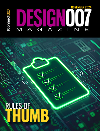
Rules of Thumb
This month, we delve into rules of thumb—which ones work, which ones should be avoided. Rules of thumb are everywhere, but there may be hundreds of rules of thumb for PCB design. How do we separate the wheat from the chaff, so to speak?
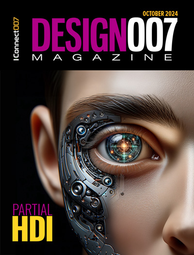
Partial HDI
Our expert contributors provide a complete, detailed view of partial HDI this month. Most experienced PCB designers can start using this approach right away, but you need to know these tips, tricks and techniques first.
Silicon to Systems: From Soup to Nuts
This month, we asked our expert contributors to weigh in on silicon to systems—what it means to PCB designers and design engineers, EDA companies, and the rest of the PCB supply chain... from soup to nuts.
- Articles
- Columns
Search Console
- Links
- Media kit
||| MENU - design007 Magazine
RUSH PCB Unveils 10-Layer HDI Design and Manufacture Capabilities
May 1, 2018 | RUSH PCBEstimated reading time: 1 minute
Rush PCB Inc. now offers the design and manufacturing of multilayer HDI PCBs of 10 layers and more.
In making the announcement, CEO Akber Roy stated, “To achieve very high-density interconnection, designers at Rush PCB Inc. use what we know as Every Layer Interconnect (ELIC) technology. This is a method wherein each layer has its own copper-filled laser-drilled microvias. When stacked up, it provides the opportunity for dynamic connections between any two layers in the PCB. Not only does this offer an increased level of flexibility, but it also maximizes circuit density.”
Roy adds that RUSH designers have taken up the additional complex challenges in routing with via-in-pad (VIP) and by employing blind and buried vias. They laser-drill via holes and filled them with conductive copper paste.
“Before finalizing the design of multi-layer PCBs, our designers confirm the structure of the circuit board primarily based on the scale, physical size, and the requirements of electromagnetic compatibility (EMC)," said Roy. "Our designers use 10 layers of material, and in this stack-up design have decided that the placement of the innerlayer and the manner of distribution of different signals in these layers of the multilayer PCB. This careful planning and determination of the stack-up design beforehand save the user much time and effort in wiring and production later.”
Roy added, “Apart from very fine traces in the foil pattern, HDI requires sequential build-up (SBU) and microvias drilled with lasers. SBU technology is used to fabricate HDI boards. The HDI layers are usually built up from a traditionally manufactured double-sided core board or multilayer PCBs.”
About RUSH PCB Inc.
Rush PCB Inc., is a printed circuit design, fabrication and assembly company located in the heart of Silicon Valley. Rush PCB engineers are experts at handling small production runs and prototypes as well as full-scale production, using both manual and automated SMD assembly processes when appropriate. RUSH can execute single and double-sided placement for all SMT component types, including BGA, UBGA, QFP, QFN, PLCC, SOIC, POP, and various other small chip packages. They can efficiently handle passive chip packages as small as 0201s, and active components with a pitch of 8 mils or more. For more information, click here.
Suggested Items
Fresh PCB Concepts: PCB Design Essentials for Electric Vehicle Charging
11/27/2024 | Team NCAB -- Column: Fresh PCB ConceptsElectric vehicles (EVs), powered by electricity rather than fossil fuels, are transforming transportation and reducing environmental impacts. But what good is an EV if it can't be easily charged? In this month's column, Ramon Roche dives into the role of printed circuit boards (PCBs) in electric vehicle charging (EVC)—and the design considerations.
Unlocking Advanced Circuitry Through Liquid Metal Ink
10/31/2024 | I-Connect007 Editorial TeamPCB UHDI technologist John Johnson of American Standard Circuits discusses the evolving landscape of electronics manufacturing and the critical role of innovation, specifically liquid metal ink technology, as an alternate process to traditional metallization in PCB fabrication to achieve ever finer features and tighter tolerances. The discussion highlights the benefits of reliability, efficiency, and yields as a tradeoff to any increased cost to run the process. As this technology becomes better understood and accepted, even sought out by customers and designers, John says there is a move toward mainstream incorporation.
Fresh PCB Concepts: The Critical Nature of Copper Thickness on PCBs
10/31/2024 | Team NCAB -- Column: Fresh PCB ConceptsPCBs are the backbone of modern electronics and the copper layers within these boards serve as the primary pathways for electrical signals. When designing and manufacturing PCBs, copper thickness is one of the most critical factors and significantly affects the board’s performance and durability. The IPC-6012F specification, the industry standard for the performance and qualification of rigid PCBs, sets clear guidelines on copper thickness to ensure reliability in different environments and applications.
Book Excerpt: The Printed Circuit Designer’s Guide to... DFM Essentials, Ch. 1
10/25/2024 | I-Connect007The guidelines offered in this book are based on both ASC recommendations and IPC standards with the understanding that some may require adjustment based on the material set, fabricator processes, and other design constraints. This chapter details high-frequency materials, copper foil types, metal core PCBs, and the benefits of embedded capacitance and resistor materials in multilayer PCBs.
The Cost-Benefit Analysis of Direct Metallization
10/21/2024 | Carmichael Gugliotti, MacDermid AlphaCarmichael Gugliotti of MacDermid Alpha discusses the innovative realm of direct metallization technology, its numerous applications, and significant advantages over traditional processes. Carmichael offers an in-depth look at how direct metallization, through developments such as Blackhole and Shadow, is revolutionizing PCB manufacturing by enhancing efficiency, sustainability, and cost-effectiveness. From its origins in the 1980s to its application in cutting-edge, high-density interconnects and its pivotal role in sustainability, this discussion sheds light on how direct metallization shapes the future of PCB manufacturing across various industries, including automotive, consumer electronics, and beyond.
Copyright © 2024 I-Connect007 | IPC Publishing Group Inc. All rights reserved.
Log in

