


 It’s Only Common Sense: Build Your Business on Reputation, Not Neglect
 The Marketing Minute: If Your Marketing Budget Gets Cut in Half, Then What?
 Punching Out: How Are the Big Boys in Electronics Doing?


One-Dimensional Material Packs a Powerful Punch for Next Generation Electronics
May 2, 2018 | University of California, RiversideEstimated reading time: 2 minutes
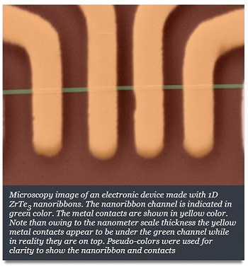
Engineers at the University of California, Riverside, have demonstrated prototype devices made of an exotic material that can conduct a current density 50 times greater than conventional copper interconnect technology.
Current density is the amount of electrical current per cross-sectional area at a given point. As transistors in integrated circuits become smaller and smaller, they need higher and higher current densities to perform at the desired level. Most conventional electrical conductors, such as copper, tend to break due to overheating or other factors at high current densities, presenting a barrier to creating increasingly small components.
The electronics industry needs alternatives to silicon and copper that can sustain extremely high current densities at sizes of just a few nanometers.
The advent of graphene resulted in a massive, worldwide effort directed at investigation of other two-dimensional, or 2D, layered materials that would meet the need for nanoscale electronic components that can sustain a high current density. While 2D materials consist of a single layer of atoms, 1D materials consist of individual chains of atoms weakly bound to one another, but their potential for electronics has not been as widely studied.
One can think of 2D materials as thin slices of bread while 1D materials are like spaghetti. Compared to 1D materials, 2D materials seem huge.
A group of researchers led by Alexander A. Balandin, a distinguished professor of electrical and computer engineering in the Marlan and Rosemary Bourns College of Engineering at UC Riverside, discovered that zirconium tritelluride, or ZrTe3, nanoribbons have an exceptionally high current density that far exceeds that of any conventional metals like copper.
The new strategy undertaken by the UC Riverside team pushes research from two-dimensional to one-dimensional materials— an important advance for the future generation of electronics.
“Conventional metals are polycrystalline. They have grain boundaries and surface roughness, which scatter electrons,” Balandin said. “Quasi-one-dimensional materials such as ZrTe3 consist of single-crystal atomic chains in one direction. They do not have grain boundaries and often have atomically smooth surfaces after exfoliation. We attributed the exceptionally high current density in ZrTe3 to the single-crystal nature of quasi-1D materials.”
In principle, such quasi-1D materials could be grown directly into nanowires with a cross-section that corresponds to an individual atomic thread, or chain. In the present study the level of the current sustained by the ZrTe3 quantum wires was higher than reported for any metals or other 1D materials. It almost reaches the current density in carbon nanotubes and graphene.
Electronic devices depend on special wiring to carry information between different parts of a circuit or system. As developers miniaturize devices, their internal parts also must become smaller, and the interconnects that carry information between parts must become smallest of all. Depending on how they are configured, the ZrTe3 nanoribbons could be made into either nanometer-scale local interconnects or device channels for components of the tiniest devices.
The UC Riverside group’s experiments were conducted with nanoribbons that had been sliced from a pre-made sheet of material. Industrial applications need to grow nanoribbon directly on the wafer. This manufacturing process is already under development, and Balandin believes 1D nanomaterials hold possibilities for applications in future electronics.
“The most exciting thing about the quasi-1D materials is that they can be truly synthesized into the channels or interconnects with the ultimately small cross-section of one atomic thread— approximately one nanometer by one nanometer,” Balandin said.
Share on:


Subscribe
Stay ahead of the technologies shaping the future of electronics with our latest newsletter, Advanced Electronics Packaging Digest. Get expert insights on advanced packaging, materials, and system-level innovation, delivered straight to your inbox.
Subscribe now to stay informed, competitive, and connected.
Suggested Items
I-Connect007 Releases The Printed Circuit Designer’s Guide to… Direct Metallization: A Guide to Complex PCB Fabrication
05/15/2026 | I-Connect007As PCB complexity continues to accelerate, fabricators and OEMs are reevaluating long-standing manufacturing processes to meet the demands of AI, HDI, advanced packaging, and next-generation electronics. To address these evolving challenges, I-Connect007 is proud to announce the release of The Printed Circuit Designer’s Guide to… Direct Metallization: A Guide to Complex PCB Fabrication, authored by MacDermid Alpha Solution’s Carmichael Gugliotti.
Driving Innovation: Selecting the Right Laser Source
04/28/2026 | Simon Khesin -- Column: Driving InnovationWhen I first joined Schmoll Maschinen, I brought experience from almost every PCB process, except for laser. As I immersed myself in laser processing, I realized why it can seem so daunting to a newcomer. The complexity arises from three intersecting factors: A vast variety of laser sources: CO2, UV-nano, green-pico, UV-pico, IR-pico, and others; a diverse range of applications: Drilling, cutting, ablation, and more; and an extensive list of materials: These have vastly different absorption rates. Choosing the right machine or laser source is rarely trivial. Even for experienced engineers, answering "Which source is best?" requires examining the business's specific goals.
Institute of Circuit Technology Spring Seminar 2026: A Bright Future in Europe
04/23/2026 | Pete Starkey, I-Connect007Through the leafy lanes and spring flowers of Warwickshire and back to Meridan, the traditional centre of England, and now officially part of the Metropolitan Borough of Solihull in the county of the West Midlands, I attended the Annual General Meeting and Spring Seminar of the Institute of Circuit Technology (ICT) on April 14. Out of the AGM came notable changes in leadership at the top of the Institute: the retirement of Mat Beadel as chair and Emma Hudson as technical director. Effective May 1, Steve Driver is the new chair, and Alun Morgan is the new technical director.
ACCM Unveils Negative and Near-zero CTE Materials for Large-Format AI Chips
04/21/2026 | Advanced Chip and Circuit MaterialsAdvanced Chip and Circuit Materials, Inc. (ACCM) has launched two new materials: Celeritas HM50, with a negative coefficient of thermal expansion (CTE) of -8 ppm/°C to offset the positive CTE and expansion of copper with temperature on circuit boards, and Celeritas HM001, with near-zero CTE and the low-loss performance needed for high-speed signal layers to 224 Gb/s and faster in artificial intelligence (AI) circuits.
Fresh PCB Concepts: Designing PCBs for Harsh Environments—Reliability Is Engineered Upstream
04/23/2026 | Team NCAB -- Column: Fresh PCB ConceptsWhen engineers hear the phrase “harsh environment,” they usually think of the extreme temperature swings, vibration and shock, pressure changes, or radiation in aerospace. However, aerospace is not the only harsh environment where electronic assemblies must survive. Automotive power electronics, downhole oil and gas tools, marine controls, rail systems, defense platforms, and industrial automation equipment all expose PCBs to environments that are equally unforgiving. The stress mechanisms may differ, but the physics does not.