


 Dan’s Biz Bookshelf: ‘Abundance: How We Build a Better Future’
 Trouble in Your Tank: In Complex Systems, Design Rules Aren’t Optional
 It’s Only Common Sense: The Phone Is Still Your Competitive Advantage


Biosensor Chip Detects Single Nucleotide Polymorphism Wirelessly and With Higher Sensitivity
July 10, 2018 | University of California San DiegoEstimated reading time: 3 minutes
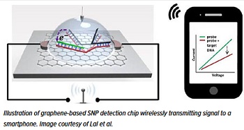
A team led by the University of California San Diego has developed a chip that can detect a type of genetic mutation known as a single nucleotide polymorphism (SNP) and wirelessly send the results in real time to a smartphone, computer, or other electronic device. The chip is at least 1,000 times more sensitive at detecting an SNP than current technology.
The advance, published July 9 in Advanced Materials, could lead to cheaper, faster and portable biosensors for early detection of genetic markers for diseases such as cancer.
An SNP is the change in a single nucleotide base (A, C, G or T) in the DNA sequence. It is the most common type of genetic mutation. While most SNPs have no discernible effect on health, some are associated with increased risk of developing pathological conditions such as cancer, diabetes, heart disease, neurodegenerative disorders, autoimmune and inflammatory diseases.
Traditional SNP detection methods have several limitations: they have relatively poor sensitivity and specificity; they require amplification to get multiple copies for detection; they require the use of bulky instruments; and they cannot work wirelessly.
The new DNA biosensor developed by the UC San Diego-led team is a wireless chip that’s smaller than a fingernail and can detect an SNP that’s present in picomolar concentrations in solution.
“Miniaturized chip-based electrical detection of DNA could enable in-field and on-demand detection of specific DNA sequences and polymorphisms for timely diagnosis or prognosis of pending health crises, including viral and bacterial infection-based epidemics,” said Ratnesh Lal, professor of bioengineering, mechanical engineering and materials science at the UC San Diego Jacobs School of Engineering.
The chip essentially captures a strand of DNA containing a specific SNP mutation and then produces an electrical signal that is sent wirelessly to a mobile device. It consists of a graphene field effect transistor with a specially engineered piece of double stranded DNA attached to the surface. This piece of DNA is bent near the middle and shaped like a pair of tweezers. One side of these so-called “DNA-tweezers” codes for a specific SNP. Whenever a DNA strand with that SNP approaches, it binds to that side of the DNA-tweezers, opening them up and creating a change in electrical current that is detected by the graphene field effect transistor.
The project is led by Lal and involves teams at the Institute of Engineering in Medicine at UC San Diego, Chinese Academy of Sciences in China, University of Pennsylvania, Max Planck Institute for Biophysical Chemistry in Germany, and Inner Mongolia Agricultural University in China.
DNA Strand Displacement
What drives this technology is a molecular process called DNA strand displacement—when a DNA double helix exchanges one of its strands for a new complementary strand. In this case, the DNA-tweezers swap one their strands for one with a particular SNP.
This is possible due to the particular way the DNA-tweezers are engineered. One of the strands is a “normal” strand that is attached to the graphene transistor and contains the complementary sequence for a specific SNP. The other is a “weak” strand in which some of the nucleotides are replaced with a different molecule to weaken its bonds to the normal strand. A strand containing the SNP is able to bind more strongly to the normal strand and displace the weak strand. This leaves the DNA-tweezers with a net electric charge that can be easily detected by the graphene transistor.
This work builds upon the first label- and amplification-free electronic SNP detection chip that Lal’s team previously developed in collaboration with Gennadi Glinksy, a research scientist at the UC San Diego Institute of Engineering in Medicine, and other UC San Diego researchers. The new chip has added wireless capability and is at least 1,000 times more sensitive than its predecessor.
What makes the new chip so sensitive is the design of the DNA-tweezers. When the SNP-containing strand binds, it opens up the DNA-tweezers, changing their geometry so that they become almost parallel to the graphene surface. This brings the net electric charge of the DNA close to the graphene surface, giving a larger signal. In contrast, the DNA probe built into the previous chip has a structure that cannot be brought closer to the graphene surface, so it generates a weaker signal upon binding an SNP-containing strand.
Next steps include designing array chips to detect up to hundreds of thousands of SNPs in a single test. Future studies will involve testing the chip on blood and other bodily fluid samples taken from animals or humans.
Share on:


Subscribe
Stay ahead of the technologies shaping the future of electronics with our latest newsletter, Advanced Electronics Packaging Digest. Get expert insights on advanced packaging, materials, and system-level innovation, delivered straight to your inbox.
Subscribe now to stay informed, competitive, and connected.
Suggested Items
Connect the Dots: Designing for the Future of Manufacturing Reality—Surface Finish
05/07/2026 | Matt Stevenson -- Column: Connect the DotsWhen designing the complex boards that many electronic devices require to operate, designers should consider manufacturability at every step. This is my last article focused on designing for the always-evolving manufacturing reality. Choosing the right surface finish has always been important. If you are creating intricate designs with a wide variety of components, like for an ultra-high density interconnect (UHDI) board, surface finish is a critical last step.
Elsyca Acquires Hivelix to Strengthen Simulation Platform for Electrochemical Surface Engineering
04/03/2026 | ElsycaElsyca, a global pioneer in computer-aided engineering (CAE) simulation for electrochemical processes and surface finishing, announces the acquisition of Hivelix, a specialist in advanced surface treatment simulation with strong expertise in multiphysics modelling and AI-assisted process optimisation.
Connect the Dots: Designing for the Future of Manufacturing Reality—Solder Mask and Legend
04/09/2026 | Matt Stevenson -- Column: Connect the DotsPCBs seem to be getting more complex by the day, so it is important for designers to keep educating themselves about the realities of manufacturing increasingly intricate boards. Last month’s column highlighted design considerations for the strip-etch-strip process and how manufacturers approach that phase of production. Now that we have a functioning board, we must protect the PCB from environmental hazards and document the circuit components. This article will detail the solder mask and legend process and offer best practices for designers to ensure a high-quality result.
Take the Mic: Photo Chemical Systems: 50 Years Strong
04/03/2026 | Real Time with... APEX EXPOPhoto Chemical Systems is celebrating 50 years in the bare board PCB market. David Graves and Jason Averette discuss how they've expanded into assembly, leveraging strong relationships and a customer-centric approach to navigate supply chain challenges. With innovative solutions and future growth strategies, including AI integration and new market ventures, Photo Chemical Systems continues enduring success.
Bold Laser Automation Introduces Precision Laser Cleaning System for Advanced Manufacturing
03/27/2026 | PRNewswireBold Laser Automation, Inc. has introduced the LPCl1820UV Laser Precision Cleaning System, a Class 1, industrial laser platform engineered for high-precision surface cleaning and thin-film removal in demanding manufacturing environments.