


 The Chemical Connection: Reducing Etch System Water Usage, Part 2
 It’s Only Common Sense: Nice Guys Really Can Finish First
 The Right Approach: I Hear the Train A Comin'
Artificial Intelligence Device Identifies Objects at the Speed of Light
August 3, 2018 | UCLAEstimated reading time: 4 minutes
A team of UCLA electrical and computer engineers has created a physical artificial neural network — a device modeled on how the human brain works — that can analyze large volumes of data and identify objects at the actual speed of light. The device was created using a 3D printer at the UCLA Samueli School of Engineering.
Numerous devices in everyday life today use computerized cameras to identify objects — think of automated teller machines that can “read” handwritten dollar amounts when you deposit a check, or internet search engines that can quickly match photos to other similar images in their databases. But those systems rely on a piece of equipment to image the object, first by “seeing” it with a camera or optical sensor, then processing what it sees into data, and finally using computing programs to figure out what it is.
The UCLA-developed device gets a head start. Called a “diffractive deep neural network,” it uses the light bouncing from the object itself to identify that object in as little time as it would take for a computer to simply “see” the object. The UCLA device does not need advanced computing programs to process an image of the object and decide what the object is after its optical sensors pick it up. And no energy is consumed to run the device because it only uses diffraction of light.
New technologies based on the device could be used to speed up data-intensive tasks that involve sorting and identifying objects. For example, a driverless car using the technology could react instantaneously — even faster than it does using current technology — to a stop sign. With a device based on the UCLA system, the car would “read” the sign as soon as the light from the sign hits it, as opposed to having to “wait” for the car’s camera to image the object and then use its computers to figure out what the object is.
Technology based on the invention could also be used in microscopic imaging and medicine, for example, to sort through millions of cells for signs of disease.
“This work opens up fundamentally new opportunities to use an artificial intelligence-based passive device to instantaneously analyze data, images and classify objects,” said Aydogan Ozcan, the study’s principal investigator and the UCLA Chancellor’s Professor of Electrical and Computer Engineering. “This optical artificial neural network device is intuitively modeled on how the brain processes information. It could be scaled up to enable new camera designs and unique optical components that work passively in medical technologies, robotics, security or any application where image and video data are essential.”
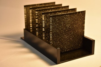
The process of creating the artificial neural network began with a computer-simulated design. Then, the researchers used a 3D printer to create very thin, 8 centimeter-square polymer wafers. Each wafer has uneven surfaces, which help diffract light coming from the object in different directions. The layers look opaque to the eye but submillimeter-wavelength terahertz frequencies of light used in the experiments can travel through them. And each layer is composed of tens of thousands of artificial neurons — in this case, tiny pixels that the light travels through.
Together, a series of pixelated layers functions as an “optical network” that shapes how incoming light from the object travels through them. The network identifies an object because the light coming from the object is mostly diffracted toward a single pixel that is assigned to that type of object.
The researchers then trained the network using a computer to identify the objects in front of it by learning the pattern of diffracted light each object produces as the light from that object passes through the device. The “training” used a branch of artificial intelligence called deep learning, in which machines “learn” through repetition and over time as patterns emerge.
“This is intuitively like a very complex maze of glass and mirrors,” Ozcan said. “The light enters a diffractive network and bounces around the maze until it exits. The system determines what the object is by where most of the light ends up exiting.”
In their experiments, the researchers demonstrated that the device could accurately identify handwritten numbers and items of clothing — both of which are commonly used tests in artificial intelligence studies. To do that, they placed images in front of a terahertz light source and let the device “see” those images through optical diffraction.
They also trained the device to act as a lens that projects the image of an object placed in front of the optical network to the other side of it — much like how a typical camera lens works, but using artificial intelligence instead of physics.
Because its components can be created by a 3D printer, the artificial neural network can be made with larger and additional layers, resulting in a device with hundreds of millions of artificial neurons. Those bigger devices could identify many more objects at the same time or perform more complex data analysis. And the components can be made inexpensively — the device created by the UCLA team could be reproduced for less than $50.
While the study used light in the terahertz frequencies, Ozcan said it would also be possible to create neural networks that use visible, infrared or other frequencies of light. A network could also be made using lithography or other printing techniques, he said.
The study’s others authors, all from UCLA Samueli, are postdoctoral scholars Xing Lin, Yair Rivenson, and Nezih Yardimci; graduate students Muhammed Veli and Yi Luo; and Mona Jarrahi, UCLA professor of electrical and computer engineering.
The research was supported by the National Science Foundation and the Howard Hughes Medical Institute. Ozcan also has UCLA faculty appointments in bioengineering and in surgery at the David Geffen School of Medicine at UCLA. He is the associate director of the UCLA California NanoSystems Institute and an HHMI professor.
Share on:


Suggested Items
Real Time with… IPC APEX EXPO 2024: Direct Imaging Equipment and Quad-wave DLP Light Engine Technology
05/03/2024 | Real Time with...IPC APEX EXPOGuest Editor Kelly Dack and MivaTek's Brendan Hogan delve into the company's innovative technologies, including direct imaging equipment and quad-wave DLP light engine technology. They highlight the benefits of direct imaging, compensation, and DART technology.
Merlin Flex invests in New Schmoll Direct Imaging System
04/30/2024 | Merlin Flex LtdMerlin Flex has fully installed and commissioned its 2nd Schmoll MDI Direct Imaging system. This new machine includes a twin bed, 4 head system which enhances Merlin Flex’s direct imaging capability for its 1.4M long flexible circuits.
Inkjet Solder Mask ‘Has Arrived’
04/10/2024 | Pete Starkey, I-Connect007I was delighted to be invited to attend an interactive webinar entitled “Solder Mask Coating Made Easy with Additive Manufacturing,” hosted by SUSS MicroTec Netherlands in Eindhoven. The webinar was introduced and moderated by André Bodegom, managing director at Adeon Technologies, and the speakers were Mariana Van Dam, senior product manager PCB imaging solutions at AGFA in Belgium; Ashley Steers, sales manager at Electra Polymers in the UK; and Dr. Luca Gautero, product manager at SUSS MicroTec Netherlands.
NetVia Group Acquires Direct Imaging from Mivatek
04/09/2024 | Miva TechnologiesMiva Technologies is pleased to announce NetVia Group, Irving, TX has acquired a new Miva 2400NG Dual Tray Direct Imaging System with 30-micron capabilities for inner, outer and soldermask imaging.
Teledyne to Acquire Adimec
02/13/2024 | TeledyneTeledyne Technologies Incorporated announced that it has entered into an agreement to acquire Adimec Holding B.V. and its subsidiaries.