


 Material Insight: The Dielectric Constant of PCB Materials
 American Made Advocacy: What About the Rest of the Technology Stack?
 It’s Only Common Sense: Great Ideas From John Mitchell’s Book on Hiring Habits
Dual-Layer Solar Cell Developed at UCLA Sets Record for Efficiently Generating Power
August 31, 2018 | UCLAEstimated reading time: 2 minutes
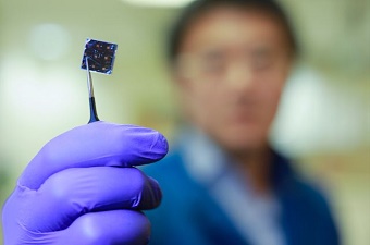
Materials scientists from the UCLA Samueli School of Engineering have developed a highly efficient thin-film solar cell that generates more energy from sunlight than typical solar panels, thanks to its double-layer design.
The device is made by spraying a thin layer of perovskite — an inexpensive compound of lead and iodine that has been shown to be very efficient at capturing energy from sunlight — onto a commercially available solar cell. The solar cell that forms the bottom layer of the device is made of a compound of copper, indium, gallium and selenide, or CIGS.
The team’s new cell converts 22.4% of the incoming energy from the sun, a record in power conversion efficiency for a perovskite–CIGS tandem solar cell. The performance was confirmed in independent tests at the U.S. Department of Energy’s National Renewable Energy Laboratory. (The previous record, set in 2015 by a group at IBM’s Thomas J. Watson Research Center, was 10.9%.) The UCLA device’s efficiency rate is similar to that of the poly-silicon solar cells that currently dominate the photovoltaics market.
“With our tandem solar cell design, we’re drawing energy from two distinct parts of the solar spectrum over the same device area,” Yang said. “This increases the amount of energy generated from sunlight compared to the CIGS layer alone.”
Yang added that the technique of spraying on a layer of perovskite could be easily and inexpensively incorporated into existing solar-cell manufacturing processes.
The cell’s CIGS base layer, which is about 2 microns (or two-thousandths of a millimeter) thick, absorbs sunlight and generates energy at a rate of 18.7% efficiency on its own, but adding the 1 micron-thick perovskite layer improves its efficiency — much like how adding a turbocharger to a car engine can improve its performance. The two layers are joined by a nanoscale interface that the UCLA researchers designed; the interface helps give the device higher voltage, which increases the amount of power it can export.
And the entire assembly sits on a glass substrate that’s about 2 millimeters thick.
“Our technology boosted the existing CIGS solar cell performance by nearly 20% from its original performance,” Yang said. “That means a 20% reduction in energy costs."
He added that devices using the two-layer design could eventually approach 30% power conversion efficiency. That will be the research group’s next goal.
The study’s lead authors are Qifeng Han, a visiting research associate in Yang’s laboratory, and Yao-Tsung Hsieh and Lei Meng, who both recently earned their doctorates at UCLA. The study’s other authors are members of Yang’s research group and researchers from Solar Frontier Corp.’s Atsugi Research Center in Japan.
The research was supported by the National Science Foundation and the Air Force Office of Scientific Research. Yang and his research group have been working on tandem solar cells for several years and their accomplishments include developing transparent tandem solar cells that could be used in windows.
Share on:


Suggested Items
DuPont Showcases AI Innovations Featuring Advanced Interconnects at 2024 International Electronic Circuits Exhibition
05/13/2024 | DuPontDuPont announced it will showcase its comprehensive range of advanced circuit materials and solutions at the 2024 International Electronic Circuits Exhibition in Shanghai. With a product portfolio that includes fine line, signal integrity, power and thermal management, DuPont will exhibit at Booth #8L06 at the National Exhibition and Convention Center (NECC) from May 13 to 15.
MKS’ Atotech to Participate in ECTC
05/10/2024 | MKS’ AtotechAt this year’s 74th IEEE Electronic Components and Technology Conference (ECTC), MKS’ Atotech will present and demonstrate its latest product and service innovations.
The Chemical Connection: Reducing Etch System Water Usage, Part 2
05/02/2024 | Don Ball -- Column: The Chemical ConnectionIn my last column, I reviewed some relatively simple ways to reduce water usage in existing etch systems: cutting down cooling coil water flow, adding chillers to replace plant water for cooling, lowering flow rate nozzles for rinses, etc. This month, I’ll continue with more ways to control water usage in your etcher. Most of these are not easily retrofittable to existing equipment but should be given serious consideration when new equipment is contemplated. With the right combination of add-ons, it is possible to bring the amount of water used in an etch system to almost zero.
Designer’s Notebook: What Designers Need to Know About Manufacturing, Part 2
04/24/2024 | Vern Solberg -- Column: Designer's NotebookThe printed circuit board (PCB) is the primary base element for providing the interconnect platform for mounting and electrically joining electronic components. When assessing PCB design complexity, first consider the component area and board area ratio. If the surface area for the component interface is restricted, it may justify adopting multilayer or multilayer sequential buildup (SBU) PCB fabrication to enable a more efficient sub-surface circuit interconnect.
Insulectro’s 'Storekeepers' Extend Their Welcome to Technology Village at IPC APEX EXPO
04/03/2024 | InsulectroInsulectro, the largest distributor of materials for use in the manufacture of PCBs and printed electronics, welcomes attendees to its TECHNOLOGY VILLAGE during this year’s IPC APEX EXPO at the Anaheim Convention Center, April 9-11, 2024.