


 It’s Only Common Sense: Would You Join Your Own Company?
 The Chemical Connection: Reducing Etch System Water Usage, Part 2
 The Right Approach: I Hear the Train A Comin'
Probing Individual Edge States With Unprecedented Precision
September 12, 2018 | University of BaselEstimated reading time: 2 minutes
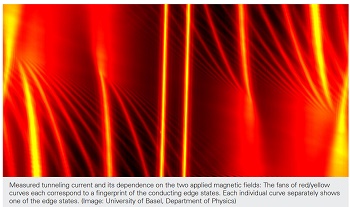
A new technique makes it possible to obtain an individual fingerprint of the current-carrying edge states occurring in novel materials such as topological insulators or 2D materials.
While insulators do not conduct electrical currents, some special materials exhibit peculiar electrical properties: though not conducting through their bulk, their surfaces and edges may support electrical currents due to quantum mechanical effects, and do so even without causing losses.
Such so-called topological insulators have attracted great interest in recent years due to their remarkable properties. In particular, their robust edge states are very promising since they could lead to great technological advances.
Currents Flowing Only Along the Edges
Similar effects as the edge states of such topological insulators also appear when a two-dimensional metal is exposed to a strong magnetic field at low temperatures. When the so-called quantum Hall effect is realized, current is thought to flow only at the edges, where several conducting channels are formed.
Probing Individual Edge States
Until now, it was not possible to address the numerous current carrying states individually or to determine their positions separately. The new technique now makes it possible to obtain an exact fingerprint of the current carrying edge states with nanometer resolution.
This is reported by researchers of the Department of Physics and the Swiss Nanoscience Institute of the University of Basel in collaboration with colleagues of the University of California, Los Angeles, as well as of Harvard and Princeton University, USA.
In order to measure the fingerprint of the conducting edge states, the physicists lead by Prof. Dominik Zumbühl have further developed a technique based on tunneling spectroscopy.
They have used a gallium arsenide nanowire located at the sample edge which runs in parallel to the edge states under investigation. In this configuration, electrons may jump (tunnel) back and forth between a specific edge state and the nanowire as long as the energies in both systems coincide. Using an additional magnetic field, the scientists control the momentum of tunneling electrons and can address individual edge states. From the measured tunneling currents, the position and evolution of each edge state may be obtained with nanometer precision.
Tracking the Evolution
This new technique is very versatile and can also be used to study dynamically evolving systems. Upon increasing the magnetic field, the number of edge states is reduced, and their distribution is modified. For the first time, the scientists were able to watch the full edge state evolution starting from their formation at very low magnetic fields.
With increasing magnetic field, the edge states are first compressed towards the sample boundary until eventually, they move towards the inside of the sample and then disappear completely. Analytical and numerical models developed by the research team agree very well with the experimental data.
“This new technique is not only very useful to study the quantum Hall edge states,” Dominik Zumbühl comments the results of the international collaboration. “It might also be employed to investigate new exotic materials such as topological insulators, graphene or other 2D materials.”
Share on:


Suggested Items
IDTechEx Discusses Low-Loss Materials: The Enabler of Future Connected Vehicles?
05/06/2024 | IDTechExFuture connected vehicles will offer future drivers a safer, smoother, and more convenient driving experience. Not only will drivers get access to more navigation and entertainment options, but they will also gain access to safety technologies that will potentially reduce accidents, improve congestion, and reduce emissions globally by allowing vehicle safety systems to communicate with each other and with city traffic infrastructure.
LQDX Divests Aluminum Soldering Business - Mina™ - to Taiyo America Inc.
05/02/2024 | PRNewswireLQDX, formerly known as Averatek Corp., developer of high-performance materials for advanced semiconductor manufacturing, today announced that it has divested its aluminum soldering business – known as MinaTM – to Taiyo America Inc., a global market leader in advanced electronic materials.
Indium Corporation Expert to Present on Pb-Free Solder for Die-Attach in Discrete Power Applications
04/30/2024 | Indium CorporationIndium Corporation Product Manager – Semiconductor Dean Payne will present at the Advanced Packaging for Power Electronics conference, hosted by IMAPS, held May 8-9 in Woburn, Massachusetts, USA.
Real Time with... IPC APEX EXPO 2024: Adhesive Materials and Equipment Update with Dymax
05/01/2024 | Real Time with...IPC APEX EXPOVirginia Hogan, global business development manager at Dymax, discusses adhesive materials, dispensing and curing equipment, a new, high-reliability conformal coating, and various materials and dispensing methods.
Real Time with... IPC APEX EXPO 2024: Sustainability in the Industry
04/26/2024 | Real Time with...IPC APEX EXPOGuest Editor Henry Crandall and Chris Nash of Indium Corporation discuss the company's 90th anniversary and its focus on sustainability. They focus on the benefits of sustainable materials, their compatibility, and value propositions. The conversation also highlights how Durafuse LT technology's role in reducing reflow temperatures is leading to significant cost and energy savings. Nash also touches on downstream sustainability efforts such as using recycled materials for packaging.