


 The Chemical Connection: Reducing Etch System Water Usage, Part 2
 It’s Only Common Sense: Nice Guys Really Can Finish First
 The Right Approach: I Hear the Train A Comin'
Metal-Organic Frameworks: Ready for Electronics
October 18, 2018 | IMDEA NanocienciaEstimated reading time: 2 minutes
Scientists have observed unequivocally for the first time band-like electron transport in an organic based material, a metal-organic framework. This semiconducting behavior, together with its cost-effective production, opens the path for employing metal organic frameworks as active materials in electronic devices.
Inorganic semiconductors as silicon, germanium or gallium arsenide are at the core of modern electronics; they are currently widely employed in e.g. computer chips, LEDs and solar cells. Inorganic semiconductors are highly pure, crystalline and hence ordered materials, these features make them good conductors of electricity under the application of an external bias (e.g. by applying a voltage). As a drawback, their high crystallinity and purity is reached by high temperature processing and then, they are very expensive to produce. A low cost alternative are organic based semiconductors as e.g. polymers, these can be procesed at room temperatures. However, the low temperature processing is generally linked with the the presence of defects and disorder in the samples. These features strongly compromise the electrical properties of organic based semiconductors; most organic based materials behave as insulators towards electrical current flow.
The scientists around group leader Enrique Cánovas (IMDEA Nanociencia and MPI-P) have now developed and characterized a novel metal-organic framework (MOF) material, an organic-based material made at room temperature that, remarkably, behaves electrically as inorganic semicondcutors. These results open the path for explotinig MOFs as active elements in electronic devices.
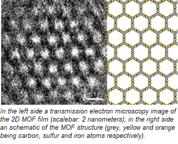
MOFs produced in the past, although crystalline, showed no or very little electrical conductivity, this was primarily due to the insulating character of the employed organic ligands coordinating the metallic centers. The new MOF, produced by Prof. Feng´s group in Dresden, is as well a highly crystalline solid, but obtained from conductive trigonal organic ligands that are coordinated by square-planar atomic metal nodes. The costituent building blocks self assemble at room temperature into a highly ordered two-dimensional (2D) semiconducting material; an atomically-thick structure. This planar geometry was expected to facilitate the transport of electrical current within the 2D plane.
The group lead by Dr. Cánovas characterized the novel 2D MOFs by Terahertz (THz) spectroscopy, a tool that measure the conductivity of a sample in ultrafast time scales (10-12 seconds), locally (measuring currents over distances as short as 10-9 meters) and optically (without the need of applying perturbative metal contacts). These aspects enabled THz spectroscopy to asses the dependence with frequency for the conductivity in the novel 2D MOF, which turns out to obey a “Drude” behaviour; the same found in e.g. in highly crystalline silicon. “From the Drude response, resolved by THz spectroscopy in the novel 2D MOFs, we infer world record electron mobilities that surpass previous values, obtained in insulating MOFs, by a factor of 10000”, says Dr. Enrique Canovas from IMDEA Nanoscience. The “Drude” behaviour implies that electrons can be displaced very easily over very long distances when a voltage is applied. These results open the path for exploiting low cost MOFs in a plethora of novel applications where long range motion of electrons is desired (e.g. in electronic devices).
This research is a joint collaboration between scientists from Germany, Bulgaria and Spain. The Technical University of Dresden, the Max Planck Institute for Polymer Research, the Max Planck Institute for Chemical Physics of Solids, the Helmholtz Zentrum in Dresden, the Wilhem-Ostwald-Institute of Physical and Theoretical Chemistry in Leipzig, The University of Sofia and the Madrid’s Institute of Advanced Studies IMDEA Nanociencia contributed to this work.
Share on:


Suggested Items
Water Management in a Large Printed Circuit Board Manufacturer
04/15/2024 | Charles Nehrig, TTM TechnologiesTTM’s environmental management is grounded in its Environmental Statement and Environmental Policy, which promote measures that make for a more responsible environmental management process. Our management system helps TTM work toward minimizing its environmental footprint and increasing the sustainability of its operations. TTM monitors its environmental performance just as it monitors its operational performance, and provides the resources required to adhere to the Company’s environmental responsibilities.
Happy’s Tech Talk #27: Integrated Mesh Power System (IMPS) for PCBs
04/08/2024 | Happy Holden -- Column: Happy’s Tech TalkA significant decrease in HDI substrate production cost can be achieved by reducing the number of substrate layers from conventional through-hole multilayers and microvia multilayers of eight, 10, 12, and more to only two layers. Besides reducing direct processing steps, the yield will increase as defect-producing operations are eliminated. The integrated mesh power system (IMPS) was invented in the latter years of MCM-D use for thin-film fabrication. Those geometries fit today into our use of ultra HDI.
Trouble in Your Tank: Supporting IC Substrates and Advanced Packaging, Part 5
03/19/2024 | Michael Carano -- Column: Trouble in Your TankDirect metallization systems based on conductive graphite or carbon dispersion are quickly gaining acceptance worldwide. Indeed, the environmental and productivity gains one can achieve with these processes are outstanding. In today’s highly competitive and litigious environment, direct metallization reduces costs associated with compliance, waste treatment, and legal issues related to chemical exposure. What makes these processes leaders in the direct metallization space?
Indium Corporation Experts to Present at SEMI THERM
03/07/2024 | Indium CorporationIndium Corporation Global Account Manager and Senior Thermal Technologist Tim Jensen and Product Development Specialist for Thermal Interface Materials Miloš Lazić will present on thermal interface material (TIM) technology at SEMI-THERM, taking place March 25–28 in San Jose, California, U.S.
Indium Corporation to Showcase Proven EV Products and High-Reliability Alloys at Productronica China
02/28/2024 | Indium CorporationAs a materials pioneer and trusted partner in electric vehicle (EV) and e-Mobility manufacturing, Indium Corporation is proud to showcase its high-reliability alloys and soldering solutions at Productronica China, March 20-22, in Shanghai.