


 The Chemical Connection: Reducing Etch System Water Usage, Part 2
 It’s Only Common Sense: Nice Guys Really Can Finish First
 The Right Approach: I Hear the Train A Comin'
Switching Identities: Revolutionary Insulator-Like Material Also Conducts Electricity
November 30, 2018 | University of Wisconsin–MadisonEstimated reading time: 3 minutes
University of Wisconsin–Madison researchers have made a material that can transition from an electricity-transmitting metal to a nonconducting insulating material without changing its atomic structure.
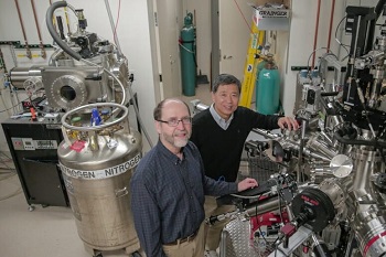
Image Caption: Chang-Beom Eom, right, and Mark Rzchowski inspect a materials growth chamber. The researchers have made a new material that can be switched from electrical conductor to insulator. UW–Madison photo by Sam Million-Weaver
“This is quite an exciting discovery,” says Chang-Beom Eom, professor of materials science and engineering. “We’ve found a new method of electronic switching.”
The new material could lay the groundwork for ultrafast electronic devices, such as the cellphones and computers of the future.
Metals like copper or silver conduct electricity, whereas insulators like rubber or glass do not allow current to flow. Some materials, however, can transition from insulating to conducting and back again.
This transition usually means that the arrangement of a material’s atoms and its conducting electrons must change in a coordinated way, but the atomic transition typically proceeds much more slowly than the smaller, lighter electrons that conduct electricity.
A material that can switch to conducting electricity like a metal without moving its atoms could dramatically advance switching speeds of advanced devices, says Eom.
“The metal-to-insulator transition is very important for switches and for logic devices with a one or a zero state,” he says. “We have the potential to use this concept to make very fast switches.”
In their research, Eom and his collaborators answered a fundamental question that has bothered scientists for years: Can the electronic and structural transition be decoupled — essentially, can the quickly changing electrons break out on their own and leave the atoms behind?
They used a material called vanadium dioxide, which is a metal when it’s heated and an insulator when it’s at room temperature. At high temperatures, the atoms that make up vanadium dioxide are arranged in a regularly repeating pattern that scientists refer to as the rutile phase. When vanadium dioxide cools down to become an insulator, its atoms adopt a different pattern, called monoclinic.
No naturally occurring substances conduct electricity when their atoms are in the monoclinic conformation. And it takes time for the atoms to rearrange when a material reaches the insulator-to-metal transition temperature.
Crucially, vanadium dioxide transitions between a metal and an insulator at different temperatures depending upon the amount of oxygen present in the material. The researchers leveraged that fact to create two thin layers of vanadium dioxide — one with a slightly lower transition temperature than the other — sandwiched on top of each other, with a sharp interface between.
When they heated the thin vanadium dioxide sandwich, one layer made the structural switch to become a metal. Atoms in the other layer remained locked into the insulating monoclinic phase. Surprisingly, however, that part of the material conducted electricity.
The new material could lay the groundwork for ultrafast electronic devices, such as the cellphones and computers of the future.
Most importantly, the material remained stable and retained its unique characteristics.
Although other research groups have attempted to create electrically conductive insulators, those materials lost their properties almost instantly — persisting for mere femtoseconds, or a few thousandths of one trillionth of a second.
The Eom team’s material, however, is here to stay.
“We were able to stabilize it, making it useful for real devices,” says Eom.
Key to their approach was the dual-layer, sandwich structure. Each layer was so thin that the interface between the two materials dominated how the entire stack behaved. It’s a notion that Eom and colleagues plan to pursue further.
“Designing interfaces could open up new materials,” says Eom.
The Wisconsin Alumni Research Foundation is assisting the researchers with patent filing.
Share on:


Suggested Items
The Chemical Connection: Reducing Etch System Water Usage, Part 2
05/02/2024 | Don Ball -- Column: The Chemical ConnectionIn my last column, I reviewed some relatively simple ways to reduce water usage in existing etch systems: cutting down cooling coil water flow, adding chillers to replace plant water for cooling, lowering flow rate nozzles for rinses, etc. This month, I’ll continue with more ways to control water usage in your etcher. Most of these are not easily retrofittable to existing equipment but should be given serious consideration when new equipment is contemplated. With the right combination of add-ons, it is possible to bring the amount of water used in an etch system to almost zero.
Designer’s Notebook: What Designers Need to Know About Manufacturing, Part 2
04/24/2024 | Vern Solberg -- Column: Designer's NotebookThe printed circuit board (PCB) is the primary base element for providing the interconnect platform for mounting and electrically joining electronic components. When assessing PCB design complexity, first consider the component area and board area ratio. If the surface area for the component interface is restricted, it may justify adopting multilayer or multilayer sequential buildup (SBU) PCB fabrication to enable a more efficient sub-surface circuit interconnect.
Insulectro’s 'Storekeepers' Extend Their Welcome to Technology Village at IPC APEX EXPO
04/03/2024 | InsulectroInsulectro, the largest distributor of materials for use in the manufacture of PCBs and printed electronics, welcomes attendees to its TECHNOLOGY VILLAGE during this year’s IPC APEX EXPO at the Anaheim Convention Center, April 9-11, 2024.
ENNOVI Introduces a New Flexible Circuit Production Process for Low Voltage Connectivity in EV Battery Cell Contacting Systems
04/03/2024 | PRNewswireENNOVI, a mobility electrification solutions partner, introduces a more advanced and sustainable way of producing flexible circuits for low voltage signals in electric vehicle (EV) battery cell contacting systems.
Heavy Copper PCBs: Bridging the Gap Between Design and Fabrication, Part 1
04/01/2024 | Yash Sutariya, Saturn Electronics ServicesThey call me Sparky. This is due to my talent for getting shocked by a variety of voltages and because I cannot seem to keep my hands out of power control cabinets. While I do not have the time to throw the knife switch to the off position, that doesn’t stop me from sticking screwdrivers into the fuse boxes. In all honesty, I’m lucky to be alive. Fortunately, I also have a talent for building high-voltage heavy copper circuit boards. Since this is where I spend most of my time, I can guide you through some potential design for manufacturability (DFM) hazards you may encounter with heavy copper design.