


 The Chemical Connection: Reducing Etch System Water Usage, Part 2
 It’s Only Common Sense: Nice Guys Really Can Finish First
 The Right Approach: I Hear the Train A Comin'
Engineers Produce Smallest 3-D Transistor Yet
December 10, 2018 | MITEstimated reading time: 5 minutes
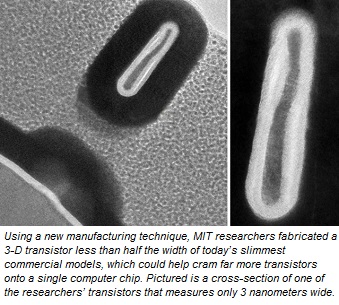
Researchers from MIT and the University of Colorado have fabricated a 3-D transistor that’s less than half the size of today’s smallest commercial models. To do so, they developed a novel microfabrication technique that modifies semiconductor material atom by atom.
The inspiration behind the work was to keep up with Moore’s Law, an observation made in the 1960s that the number of transistors on an integrated circuit doubles about every two years. To adhere to this “golden rule” of electronics, researchers are constantly finding ways to cram as many transistors as possible onto microchips. The newest trend is 3-D transistors that stand vertically, like fins, and measure about 7 nanometers across — tens of thousands of times thinner than a human hair. Tens of billions of these transistors can fit on a single microchip, which is about the size of a fingernail.
As described in a paper presented at this week’s IEEE International Electron Devices Meeting, the researchers modified a recently invented chemical-etching technique, called thermal atomic level etching (thermal ALE), to enable precision modification of semiconductor materials at the atomic level. Using that technique, the researchers fabricated 3-D transistors that are as narrow as 2.5 nanometers and more efficient than their commercial counterparts.
Similar atomic-level etching methods exist today, but the new technique is more precise and yields higher-quality transistors. Moreover, it repurposes a common microfabrication tool used for depositing atomic layers on materials, meaning it could be rapidly integrated. This could enable computer chips with far more transistors and greater performance, the researchers say.
“We believe that this work will have great real-world impact,” says first author Wenjie Lu, a graduate student in MIT’s Microsystems Technology Laboratories (MTL). “As Moore’s Law continues to scale down transistor sizes, it is harder to manufacture such nanoscale devices. To engineer smaller transistors, we need to be able to manipulate the materials with atomic-level precision.”
Joining Lu on the paper are: Jesus A. del Alamo, a professor of electrical engineering and computer science and an MTL researcher who leads the Xtreme Transistors Group; recent MIT graduate Lisa Kong ’18; MIT postdoc Alon Vardi; and Jessica Murdzek, Jonas Gertsch, and Professor Steven George of the University of Colorado.
Atom by Atom
Microfabrication involves deposition (growing film on a substrate) and etching (engraving patterns on the surface). To form transistors, the substrate surface gets exposed to light through photomasks with the shape and structure of the transistor. All material exposed to light can be etched away with chemicals, while material hidden behind the photomask remains.
The state-of-the-art techniques for microfabrication are known as atomic layer deposition (ALD) and atomic layer etching (ALE). In ALD, two chemicals are deposited onto the substrate surface and react with one another in a vacuum reactor to form a film of desired thickness, one atomic layer at a time.
Traditional ALE techniques use plasma with highly energetic ions that strip away individual atoms on the material’s surface. But these cause surface damage. These methods also expose material to air, where oxidization causes additional defects that hinder performance.
In 2016, the University of Colorado team invented thermal ALE, a technique that closely resembles ALD and relies on a chemical reaction called “ligand exchange.” In this process, an ion in one compound called a ligand — which binds to metal atoms — gets replaced by a ligand in a different compound. When the chemicals are purged away, the reaction causes the replacement ligands to strip away individual atoms from the surface. Still in its infancy, thermal ALE has, so far, only been used to etch oxides.
In this new work, the researchers modified thermal ALE to work on a semiconductor material, using the same reactor reserved for ALD. They used an alloyed semiconductor material, called indium gallium arsenide (or InGaAs), which is increasingly being lauded as a faster, more efficient alternative to silicon.
The researchers exposed the material to hydrogen fluoride, the compound used for the original thermal ALE work, which forms an atomic layer of metal fluoride on the surface. Then, they poured in an organic compound called dimethylaluminum chloride (DMAC). The ligand-exchange process occurs on the metal fluoride layer. When the DMAC is purged, individual atoms follow.
The technique is repeated over hundreds of cycles. In a separate reactor, the researchers then deposited the “gate,” the metallic element that controls the transistors to switch on or off.
In experiments, the researchers removed just .02 nanometers from the material’s surface at a time. “You’re kind of peeling an onion, layer by layer,” Lu says. “In each cycle, we can etch away just 2 percent of a nanometer of a material. That gives us super high accuracy and careful control of the process.”
Because the technique is so similar to ALD, “you can integrate this thermal ALE into the same reactor where you work on deposition,” del Alamo says. It just requires a “small redesign of the deposition tool to handle new gases to do deposition immediately after etching. … That’s very attractive to industry.”
Page 1 of 2
Share on:


Suggested Items
LQDX Divests Aluminum Soldering Business - Mina™ - to Taiyo America Inc.
05/02/2024 | PRNewswireLQDX, formerly known as Averatek Corp., developer of high-performance materials for advanced semiconductor manufacturing, today announced that it has divested its aluminum soldering business – known as MinaTM – to Taiyo America Inc., a global market leader in advanced electronic materials.
Indium Corporation Expert to Present on Pb-Free Solder for Die-Attach in Discrete Power Applications
04/30/2024 | Indium CorporationIndium Corporation Product Manager – Semiconductor Dean Payne will present at the Advanced Packaging for Power Electronics conference, hosted by IMAPS, held May 8-9 in Woburn, Massachusetts, USA.
Real Time with... IPC APEX EXPO 2024: Adhesive Materials and Equipment Update with Dymax
05/01/2024 | Real Time with...IPC APEX EXPOVirginia Hogan, global business development manager at Dymax, discusses adhesive materials, dispensing and curing equipment, a new, high-reliability conformal coating, and various materials and dispensing methods.
Real Time with... IPC APEX EXPO 2024: Sustainability in the Industry
04/26/2024 | Real Time with...IPC APEX EXPOGuest Editor Henry Crandall and Chris Nash of Indium Corporation discuss the company's 90th anniversary and its focus on sustainability. They focus on the benefits of sustainable materials, their compatibility, and value propositions. The conversation also highlights how Durafuse LT technology's role in reducing reflow temperatures is leading to significant cost and energy savings. Nash also touches on downstream sustainability efforts such as using recycled materials for packaging.
SMC Korea 2024 to Highlight Semiconductor Materials Trends and Innovations on Industry’s Path to $1 Trillion
04/24/2024 | SEMIWith Korea a major consumer of semiconductor materials and advanced materials a key driver of innovation on the industry’s path to $1 trillion, industry leaders and experts will gather at SMC (Strategic Materials Conference) Korea 2024 on May 29 at the Suwon Convention Center in Gyeonggi-do, South Korea to provide insights into the latest materials developments and trends. Registration is open.