


 The Chemical Connection: Reducing Etch System Water Usage, Part 2
 It’s Only Common Sense: Nice Guys Really Can Finish First
 The Right Approach: I Hear the Train A Comin'
Nanotopography of an Atomic World
January 16, 2019 | Pennsylvania State UniversityEstimated reading time: 3 minutes
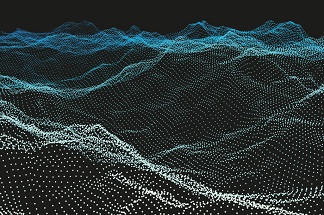
Physicists offer insights into the structure of atomically thin materials using nanoscale images of 2D membranes.
Nanoscale materials are at the forefront of solving some of the world’s biggest engineering challenges. With everything from super-light bicycles to quantum electronics made possible with nanotechnology, researchers are eager to tap into the vast potential of these materials.
But scaling things up from an atomic level is a monumental task, and making usable amounts of nanoscale materials continues to be a significant hurdle for materials scientists and engineers.
Now, researchers in Penn’s Department of Physics & Astronomy are paving the way for the future of nanomaterial applications by providing insights into how these thin 2D membranes form. The study from the lab of Marija Drndić, published in the journal Nano Letters, also offers a view of what these materials look like at the nanometer scale.
The study builds on previous work done by the Drndić lab and focuses on a “less attractive” form of 2D membranes. Most research in the field focuses on membranes that are comprised of a monolayer that is only one atom thick. In this study, the Drndić lab used membranes that have a mix of thicknesses. In some areas of the membrane, the thickness is only one or two atoms, while in others membranes are about 10 atoms thick.
These membranes are considered “less attractive” because they may not be ideal for applications such as electronics. However, these membranes are strong, versatile, and much easier to make in the lab. “This additional robustness can be used for applications like desalination or gas transport,” says Priyanka Thiruraman, a graduate student involved with the study.
Making this kind of porous 2D membrane requires three steps. The first is to grow the membranes on sheets of molybdenum foil by heating them to 800°C (about 1470°F) in a chamber with sulfur vapor. This process creates the 2D membrane, which is made of molybdenum bound with sulfur.
The second step is to add atomic-scale holes to the membrane using a process called acid etching. Both the growing and the etching can be finished in a single day. “You don’t need any special chemicals to make these membranes,” says Paul Masih Das, a graduate student who was the lead author of this study. “You could even make them in your basement.”
The third step is where this work goes from something you could do in your basement to cutting-edge physics research. It’s also what makes this particular study so impactful.
Using a scanning transmission electron microscope, Masih Das was able to take pictures of these membranes at an atomic scale, bringing to life the shape of these membranes through “nanotopography.” The images show the layout of individual atoms within the membrane and reveal patterns that resemble a map of atomic hills and valleys. “This level of structure, where we can see the individual atoms of these multilayer molybdenum disulfide membranes, hasn’t been seen in the related literature before,” says Drndić.
Masih Das said that these results were unexpected; they thought they would find a structure that was more uniform and grid-like. It’s unexpected results like this that drive the Drndić lab to keep exploring the potential of how these “less attractive” materials could be used in the future.
“The idea of desalination came naturally. It’s not that we planned it; it was just that for the holes that we were making for DNA sequencing applications we noticed that if they were smaller then we can filter ions. When we first published on that topic, there were not many papers at all out there. Now, all of a sudden, there are many more papers, and there’s more of a research community.”
The Drndić lab continues to study the fundamental nature of 2D membranes and other nanomaterials. “We let it grow naturally,” Drndić says about the work done in her lab. “If we see another opportunity, we might jump on it. It’s nice to have that kind of freedom, where you’re not under pressure to always justify the cost or the application. It’s nice to be able to just explore and to bump onto new things.”
Share on:


Suggested Items
LQDX Divests Aluminum Soldering Business - Mina™ - to Taiyo America Inc.
05/02/2024 | PRNewswireLQDX, formerly known as Averatek Corp., developer of high-performance materials for advanced semiconductor manufacturing, today announced that it has divested its aluminum soldering business – known as MinaTM – to Taiyo America Inc., a global market leader in advanced electronic materials.
Indium Corporation Expert to Present on Pb-Free Solder for Die-Attach in Discrete Power Applications
04/30/2024 | Indium CorporationIndium Corporation Product Manager – Semiconductor Dean Payne will present at the Advanced Packaging for Power Electronics conference, hosted by IMAPS, held May 8-9 in Woburn, Massachusetts, USA.
Real Time with... IPC APEX EXPO 2024: Adhesive Materials and Equipment Update with Dymax
05/01/2024 | Real Time with...IPC APEX EXPOVirginia Hogan, global business development manager at Dymax, discusses adhesive materials, dispensing and curing equipment, a new, high-reliability conformal coating, and various materials and dispensing methods.
Real Time with... IPC APEX EXPO 2024: Sustainability in the Industry
04/26/2024 | Real Time with...IPC APEX EXPOGuest Editor Henry Crandall and Chris Nash of Indium Corporation discuss the company's 90th anniversary and its focus on sustainability. They focus on the benefits of sustainable materials, their compatibility, and value propositions. The conversation also highlights how Durafuse LT technology's role in reducing reflow temperatures is leading to significant cost and energy savings. Nash also touches on downstream sustainability efforts such as using recycled materials for packaging.
SMC Korea 2024 to Highlight Semiconductor Materials Trends and Innovations on Industry’s Path to $1 Trillion
04/24/2024 | SEMIWith Korea a major consumer of semiconductor materials and advanced materials a key driver of innovation on the industry’s path to $1 trillion, industry leaders and experts will gather at SMC (Strategic Materials Conference) Korea 2024 on May 29 at the Suwon Convention Center in Gyeonggi-do, South Korea to provide insights into the latest materials developments and trends. Registration is open.