


 Happy’s Tech Talk #28: The Power Mesh Architecture for PCBs
 It’s Only Common Sense: Would You Join Your Own Company?
 The Chemical Connection: Reducing Etch System Water Usage, Part 2
Causes for Defects in 3D Printing and Paves Way for Better Results
February 22, 2019 | PRNewswireEstimated reading time: 6 minutes
Additive manufacturing's promise to revolutionize industry is constrained by a widespread problem: tiny gas pockets in the final product, which can lead to cracks and other failures.
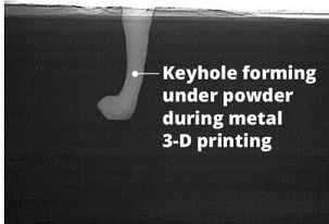
This image, taken under the synchrotron at Argonne National Laboratory, shows a keyhole void forming during the metal 3-D printing process. During laser powder bed fusion, a 3-D printer “drills” a hole into the metal.
New research published today in Science, led by researchers from Carnegie Mellon University and Argonne National Laboratory, has identified how and when these gas pockets form, as well as a methodology to predict their formation—a pivotal discovery that could dramatically improve the 3D printing process.
"The research in this paper will translate into better quality control and better control of working with the machines," said Anthony Rollett, a Professor of Materials Science and Engineering at Carnegie Mellon University and an author on the paper. "For additive manufacturing to really take off for the majority of companies, we need to improve the consistency of the finished products. This research is a major step in that direction."
The scientists used the extremely bright high-energy X-rays at Argonne's Advanced Photon Source (APS), a DOE Office of Science User Facility, to take super-fast video and images of a process called Laser Power Bed Fusion (LPBF), in which lasers are used to melt and fuse material powder together.
The lasers, which scan over each layer of powder to fuse metal where it is needed, literally create the finished product from the ground up. Defects can form when pockets of gas become trapped into these layers, causing imperfections that could lead to cracks or other breakdowns in the final product.
Until now, manufacturers and researchers did not know much about how the laser drills into the metal, producing cavities called "vapor depressions," but they assumed that the type of metal powder or strength of laser were to blame. As a result, manufacturers have been using a trial and error approach with different types of metals and lasers to seek to reduce the defects.
In fact, the research shows that these vapor depressions exist under nearly all conditions in the process, no matter the laser or metal. Even more important, the research shows how to predict when a small depression will grow into a big and unstable one that can potentially create a defect.
"We're drawing back the veil and revealing what's really going on," Rollett said. "Most people think you shine a laser light on the surface of a metal powder, the light is absorbed by the material, and it melts the metal into a melt pool. In actuality, you're really drilling a hole into the metal."
By using highly specialized equipment at Argonne's APS, one of the most powerful synchrotron facilities in the world, researchers watched what happens as the laser moves across the metal powder bed to create each layer of the product.
Under perfect conditions, the melt pool shape is shallow and semicircular, called the "conduction mode." But during the actual printing process, the high-power laser, often moving at a low speed, can change the melt pool shape to something like a keyhole in a warded lock: round and large on top, with a narrow spike at bottom. Such "keyhole mode" melting can potentially lead to defects in the final product.
"Based on this research, we now know that the keyhole phenomenon is more important, in many ways, than the powder being used in additive manufacturing," said Ross Cunningham, a recent graduate from Carnegie Mellon University and one of the co-first authors of this paper. "Our research shows that you can predict the factors that lead to a keyhole—which means you can also isolate those factors for better results."
The research shows that keyholes form when a certain laser power density is reached that is sufficient to boil the metal. This, in turn, reveals the critical importance of the laser focus in the additive manufacturing process, an element that has received scant attention so far, according to the research team.
"The keyhole phenomenon was able to be viewed for the first time with such details because of the scale and specialized capability developed at Argonne," said Tao Sun, an Argonne physicist and an author on the paper. "The intense high-energy X-ray beam at the APS is key to discoveries like this."
The experiment platform that supports study of additive manufacturing includes a laser apparatus, specialized detectors, and dedicated beamline instruments.
Page 1 of 2
Share on:


Suggested Items
Connect the Dots: Designing for Reality—The Pre-Manufacturing Process
05/08/2024 | Matt Stevenson -- Column: Connect the DotsI have been working with Nolan Johnson on a podcast series about designing PCBs for the reality of manufacturing. By sharing lessons learned over a long career in the PCB industry, we hope to shorten learning curves and help designers produce better boards with less hassle and rework. Episode 2 deals with the electronic pre-manufacturing process. Moving from CAD (computer-aided design) to CAM (computer-aided manufacturing) is a key step in PCB manufacturing. CAM turns digital designs into instructions that machines can use to actually build the PCB.
All Flex Solutions Hires Mike Madetzke as Manager of R&D
05/08/2024 | All Flex SolutionsAll Flex Solutions is very pleased to announce that Mike Madetzke has joined their team as their new Manager of Research and Development.
Shane Whiteside of Summit Reflects on Today's PCB Landscape
05/08/2024 | I-Connect007 Editorial TeamSummit Interconnect began as a printed circuit board manufacturing company just eight years ago and has seen impressive growth organically and through acquisition. Summit President and CEO Shane Whiteside takes a few moments to share his thoughts on the growing PCB industry in the United States.
America Projected to Triple Semiconductor Manufacturing Capacity by 2032, the Largest Rate of Growth in the World
05/08/2024 | SIAThe Semiconductor Industry Association (SIA), in partnership with the Boston Consulting Group (BCG), released a report on the global chip supply chain that projects the United States will triple its domestic semiconductor manufacturing capacity from 2022—when the CHIPS and Science Act (CHIPS) was enacted—to 2032.
Coherix Partners with EMU on 'Factory of the Future' Technology Program
05/08/2024 | PRNewswireMichigan-based Coherix is working with Eastern Michigan University (EMU) in Ypsilanti to develop "factory-of-the-future" manufacturing and assembly technology.