


 The Chemical Connection: Reducing Etch System Water Usage, Part 2
 It’s Only Common Sense: Nice Guys Really Can Finish First
 The Right Approach: I Hear the Train A Comin'
Scientists Develop Printable Water Sensor
March 5, 2019 | DESYEstimated reading time: 3 minutes
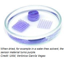
A new, versatile plastic-composite sensor can detect tiny amounts of water. The 3D printable material, developed by a Spanish-Israeli team of scientists, is cheap, flexible and non-toxic and changes its colour from purple to blue in wet conditions. The researchers lead by Pilar Amo-Ochoa from the Autonomous University of Madrid (UAM) used DESY’s X-ray light source PETRA III to understand the structural changes within the material that are triggered by water and lead to the observed colour change. The development opens the door to the generation of a family of new 3D printable functional materials, as the scientists write in the journal Advanced Functional Materials (early online view).
In many fields, from health to food quality control, environmental monitoring and technical applications, there is a growing demand for responsive sensors which show fast and simple changes in the presence of specific molecules. Water is among the most common chemicals to be monitored. “Understanding how much water is present in a certain environment or material is important,” explains DESY scientist Michael Wharmby, co-author of the paper and head of beamline P02.1 where the sensor-material was examined with X-rays. “For example, if there is too much water in oils they may not lubricate machines well, whilst with too much water in fuel, it may not burn properly.”
The functional part of the scientists’ new sensor-material is a so-called copper-based coordination polymer, a compound with a water molecule bound to a central copper atom. “On heating the compound to 60 degrees Celsius, it changes colour from blue to purple”, reports Pilar Amo-Ochoa. “This change can be reversed by leaving it in air, putting it in water, or putting it in a solvent with trace amounts of water in it.” Using high-energy X-rays from DESY's research light source PETRA III at the experimental station P02.1, the scientists were able to see that in the sample heated to 60 degrees Celsius, the water molecule bound to the copper atoms had been removed. This leads to a reversible structural reorganisation of the material, which is the cause of the colour change.
“Having understood this, we were able to model the physics of this change,” explains co-author José Ignacio Martínez from the Institute for Materials Science in Madrid (ICMM-CSIC). The scientists were then able to mix the copper compound into a 3D printing ink and printed sensors in several different shapes which they tested in air and with solvents containing different amounts of water. These tests showed that the printed objects are even more sensitive to the presence of water than the compound by itself, thanks to their porous nature. In solvents, the printed sensors could already detect 0.3 to 4 per cent of water in less than two minutes. In air, they could detect a relative humidity of 7 per cent.
If it is dried, either in a water free solvent or by heating, the material turns back to purple. A detailed investigation showed that the material is stable even over many heating cycles, and the copper compounds are evenly distributed throughout the printed sensors. Also, the material is stable in air over at least one year and also at biological relevant pH ranges from 5 to 7. “Furthermore, the highly versatile nature of modern 3D printing means that these devices could be used in a huge range of different places,” emphasises co-author Shlomo Magdassi from The Hebrew University of Jerusalem. He adds that the concept could be used to develop other functional materials as well.
“This work shows the first 3D printed composite objects created from a non-porous coordination polymer,” says co-author Félix Zamora from the Autonomous University of Madrid. “It opens the door to the use of this large family of compounds that are easy to synthesize and exhibit interesting magnetic, conductive and optical properties, in the field of functional 3D printing.”
The Autonomous University of Madrid, the Hebrew University of Jerusalem, the Nanyang Technological University in Singapore, the Institute for Materials Science in Madrid and DESY contributed to this research.
Share on:


Suggested Items
The Chemical Connection: Reducing Etch System Water Usage, Part 2
05/02/2024 | Don Ball -- Column: The Chemical ConnectionIn my last column, I reviewed some relatively simple ways to reduce water usage in existing etch systems: cutting down cooling coil water flow, adding chillers to replace plant water for cooling, lowering flow rate nozzles for rinses, etc. This month, I’ll continue with more ways to control water usage in your etcher. Most of these are not easily retrofittable to existing equipment but should be given serious consideration when new equipment is contemplated. With the right combination of add-ons, it is possible to bring the amount of water used in an etch system to almost zero.
Designer’s Notebook: What Designers Need to Know About Manufacturing, Part 2
04/24/2024 | Vern Solberg -- Column: Designer's NotebookThe printed circuit board (PCB) is the primary base element for providing the interconnect platform for mounting and electrically joining electronic components. When assessing PCB design complexity, first consider the component area and board area ratio. If the surface area for the component interface is restricted, it may justify adopting multilayer or multilayer sequential buildup (SBU) PCB fabrication to enable a more efficient sub-surface circuit interconnect.
Insulectro’s 'Storekeepers' Extend Their Welcome to Technology Village at IPC APEX EXPO
04/03/2024 | InsulectroInsulectro, the largest distributor of materials for use in the manufacture of PCBs and printed electronics, welcomes attendees to its TECHNOLOGY VILLAGE during this year’s IPC APEX EXPO at the Anaheim Convention Center, April 9-11, 2024.
ENNOVI Introduces a New Flexible Circuit Production Process for Low Voltage Connectivity in EV Battery Cell Contacting Systems
04/03/2024 | PRNewswireENNOVI, a mobility electrification solutions partner, introduces a more advanced and sustainable way of producing flexible circuits for low voltage signals in electric vehicle (EV) battery cell contacting systems.
Heavy Copper PCBs: Bridging the Gap Between Design and Fabrication, Part 1
04/01/2024 | Yash Sutariya, Saturn Electronics ServicesThey call me Sparky. This is due to my talent for getting shocked by a variety of voltages and because I cannot seem to keep my hands out of power control cabinets. While I do not have the time to throw the knife switch to the off position, that doesn’t stop me from sticking screwdrivers into the fuse boxes. In all honesty, I’m lucky to be alive. Fortunately, I also have a talent for building high-voltage heavy copper circuit boards. Since this is where I spend most of my time, I can guide you through some potential design for manufacturability (DFM) hazards you may encounter with heavy copper design.